Light Emitting Element and Light Emitting Device Using the Same

a technology of light emitting elements and light emitting devices, applied in the direction of organic semiconductor devices, other domestic articles, natural mineral layered products, etc., can solve the problem of increasing the driving voltage, and achieve the effects of increasing resistance, high reliability, and slight increase in driving voltag

Active Publication Date: 2008-10-02
SEMICON ENERGY LAB CO LTD
View PDF23 Cites 41 Cited by
  • Summary
  • Abstract
  • Description
  • Claims
  • Application Information

AI Technical Summary

Benefits of technology

[0013]A highly reliable light emitting element having slight increase in driving voltage with the accumulation of light emitting time can be obtained in accordance with the present invention.
[0014]In addition, a light emitting element having slight increase in resistance that is dependent on the thickness of a layer generating holes can be obtained. As a result, a light emitting element in that a distance between electrodes can be easily changed can be obtained. By increasing the distance between the electrodes, the short-circuiting between the electrodes caused by the unevenness on the surfaces of the electrodes can be prevented. Also, by adjusting the distance between the electrodes, an optical distance can be easily adjusted so as to maximize an light extraction efficiency easily. Furthermore, by adjusting the distance between the electrodes, the optical distance can be controlled easily so that the variation in emission spectrum depending on an angle of seeing a light emitting surface is reduced.
[0015]Furthermore, by applying the light emitting element obtained in accordance with the present invention to a light emitting device, a highly reliable light emitting device that can withstand long-time use can be obtained. Moreover, by applying the light emitting element obtained in accordance with the present invention to a light emitting device having a display function, it is possible to obtain a light emitting device capable of displaying high-definition images with slight variation in the emission spectrum that depends on an angle of seeing a light emitting surface, wherein light can be emitted to the outside efficiently.

Problems solved by technology

Many of these light emitting elements have a problem that the driving voltage is increased in accordance with the accumulation of light emitting time.

Method used


Image

  • Light Emitting Element and Light Emitting Device Using the Same
  • Light Emitting Element and Light Emitting Device Using the Same
  • Light Emitting Element and Light Emitting Device Using the Same

Examples


embodiment mode 1

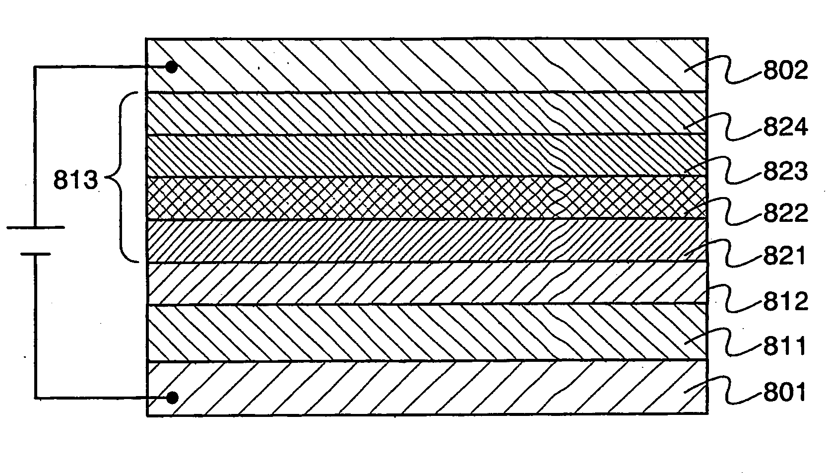
[0030]One embodiment mode of the present invention will be described with reference to a cross sectional view of a light emitting element as shown in FIG. 1.

[0031]A first layer 811, a second layer 812, and a third layer 813 are interposed between a first electrode 801 and a second electrode 802. The first layer 811, the 6 second layer 812 and the third layer 813 are sequentially laminated. The first layer 811 is in contact with the first electrode 801 while the third layer 813 is in contact with the second electrode 802.

[0032]The light emitting element of the present embodiment mode is operated as follows. Upon applying a voltage to the light emitting element such that a potential of the second electrode 802 is higher than that of the first electrode 801, holes are injected in the first electrode 801 from the first layer 811 while electrons are injected in the third layer 813 from the second layer 812. Also, holes are injected in the third layer 813 from the second electrode 802. Th...

embodiment mode 2

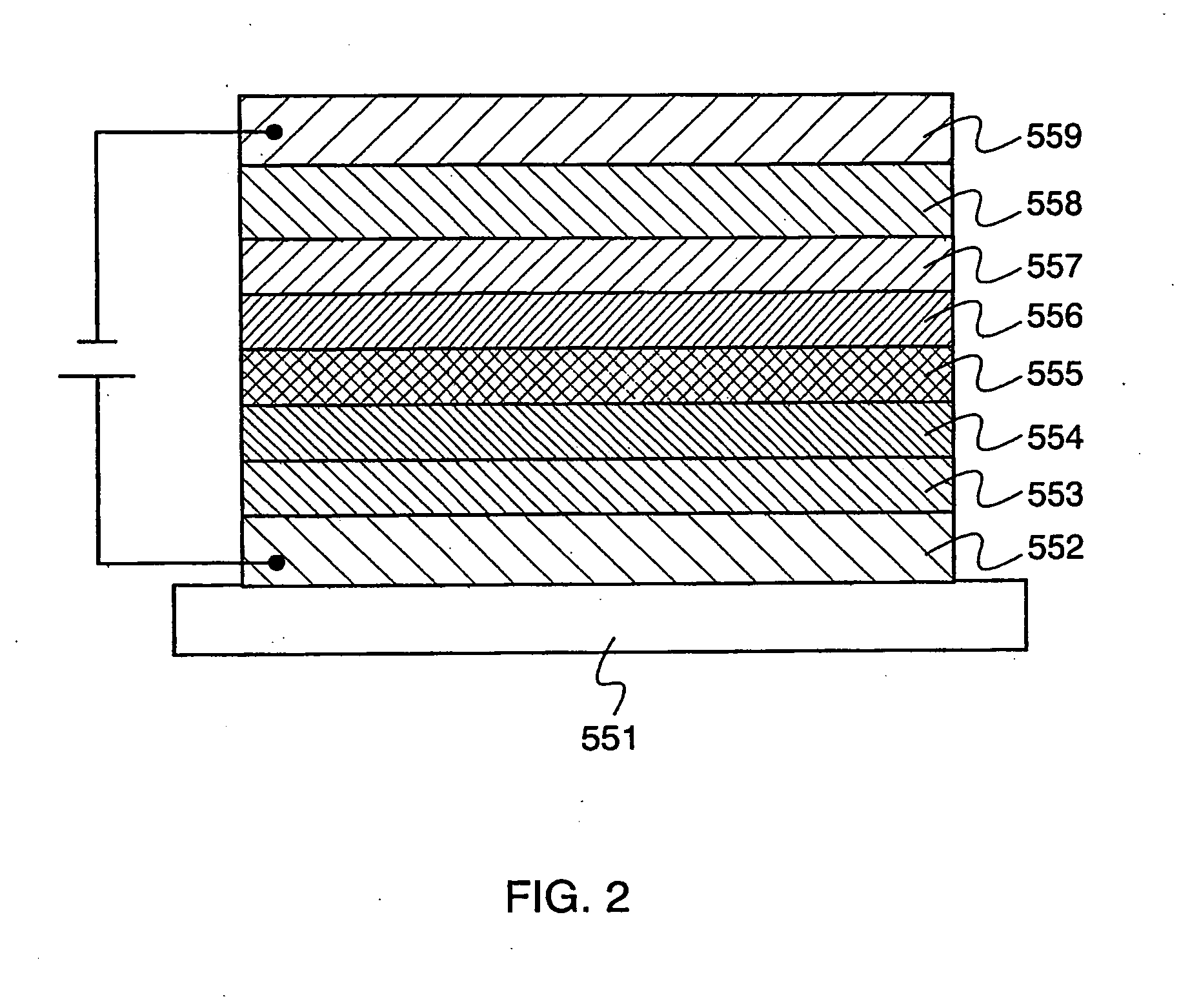
[0058]This embodiment mode will describe a light emitting element in which a light extraction efficiency is increased by controlling the thickness of a layer generating holes and an optical distance between a reflecting surface and a light emitting surface (or a light emitting region) is controlled to reduce the change in emission spectrum depending on an angle of seeing the light emitting surface, with reference to FIG. 12.

[0059]A light emitting element of FIG. 12 comprises a first layer 211 generating holes, a second layer 212 generating electrons and a third layer 213 containing a light emitting substance between a first electrode 201 and a second electrode 202. The first layer 211, the second layer 212 and the third layer 213 are sequentially laminated while sandwiching the second layer 212 between the first and third layers. The first layer 211 is in contact with the first electrode while the third layer 213 is in contact with the second electrode 202.

[0060]The first electrode ...

embodiment mode 3

[0074]The light emitting element according to the present invention is a highly reliable element having slight increase in the driving voltage with the accumulation of light emitting time. By applying the light emitting element of the invention to, e.g., a pixel portion, a light emitting device having low power consumption can be obtained. Also, the light emitting element of the invention can prevent the short-circuiting between electrodes easily. Therefore, by applying the light emitting element of the invention to a pixel portion, a light emitting device capable of displaying favorable images having less defects due to the short-circuiting can be obtained. Furthermore, the light emitting element in accordance with the invention can easily emit light to the outside. By applying the light emitting element of the invention to a pixel portion, a light emitting device that can perform display operation at low power consumption can be obtained.

[0075]In this embodiment mode, circuit stru...


PUM

PropertyMeasurementUnit
molar ratioaaaaaaaaaa

Abstract

An object of the prevent invention is to provide a light emitting element having slight increase in driving voltage with accumulation of light emitting time. Another object of the invention is to provide a light emitting element having slight increase in resistance with increase in film thickness. In an aspect of the invention, a light emitting element includes first, second and layers between mutually-facing first and second electrodes. The first layer is provided to be closer to the first electrode than the second layer. The third layer is provided to be closer to the second electrode than the second layer. The first layer contains a bipolar substance and a substance exhibiting an electron accepting ability with respect to the bipolar substance. The second layer contains a bipolar substance and a substance exhibiting an electron donating ability with respect to the bipolar substance. The third layer contains a light emitting substance.

Description

TECHNICAL FIELD[0001]The present invention relates to a light emitting element including a light emitting substance between a pair of electrodes, and in particular, relates to the structure of the light emitting element.BACKGROUND ART[0002]In recent years, many of light emitting elements used for a display device and the like have a structure in that a light emitting substance is interposed between a pair of electrodes. In a light emitting element having such a structure, when returning an exciton that is formed by recombination of an electron injected from one electrode and a hole injected from the other electrode to a ground state, light is emitted. Many of these light emitting elements have a problem that the driving voltage is increased in accordance with the accumulation of light emitting time.[0003]As one example for solving this problem, for example, the patent document 1 discloses an organic EL element, wherein increase in the driving voltage in driving the organic EL elemen...

Claims


Application Information

Patent Timeline
Patent Type & Authority Applications(United States)
IPC IPC(8): H05B33/14
CPCH01L27/3244H01L27/3281H01L51/006H01L51/0061H01L51/50H01L51/5088H01L51/5092H01L51/5262H01L2251/558Y10S428/917H10K59/17H10K59/12H10K85/636H10K85/633H10K50/17H10K50/171H10K50/00H10K50/85H10K2102/351H10K85/631H10K10/82H10K50/15H10K50/16H10K50/11
Inventor KUMAKI, DAISUKESEO, SATOSHI
Owner SEMICON ENERGY LAB CO LTD
Why Eureka
Try Eureka