Direct-conversion transmitter circuit and transceiver system

a transmitter circuit and direct-conversion technology, applied in the direction of automatic tone/bandwidth control, substation equipment, gain control, etc., can solve the problems of difficult to apply to a modulation system in which information is used, and achieve the effect of large variable width

Inactive Publication Date: 2007-06-21
RENESAS ELECTRONICS CORP
View PDF16 Cites 39 Cited by
  • Summary
  • Abstract
  • Description
  • Claims
  • Application Information

AI Technical Summary

Benefits of technology

[0013] The present invention may provide a transmitter circuit having variable width of broad output level of 70 dB or higher without necessitating any expensive exterior high-frequency filter such as SAW (Surface Acoustic Wave) which inhibits cost reduction in order to further reduce the cost and reduce a number of components. Also, the present invention may provide a transmitter and a transceiver system using the transmitter circuit.
[0017] In other words, briefly speaking, a transmitter circuit according to the present invention is constructed such that a direct conversion system is used for the transmitter circuit, there is provided variable gain means in an input portion of an orthogonal modulator and bias of the orthogonal modulator is changed in interlock with a change in gain. Thereby, it is possible to realize large variable width while a ratio of carrier leak to a transmission signal is maintained.

Problems solved by technology

Although the offset PLL has been broadly applied without necessitating any exterior filter for high frequency as described above, it has been difficult to apply to a modulation system in which information is included even in such a change in amplitude as HQPSK (Hybrid Quadrature Phase Shift Keying) which has been adopted in W-CDMA (Wideband CDMA (Code Division Multiple Access).
Also, it has been difficult to realize a change in signal level of 70 dB or higher which is requested in the W-CDMA.

Method used


Image

  • Direct-conversion transmitter circuit and transceiver system
  • Direct-conversion transmitter circuit and transceiver system
  • Direct-conversion transmitter circuit and transceiver system

Examples


first embodiment

[0036] With reference to FIGS. 1 to 4, the description will be made of the first embodiment of the present invention. First, the description will be made of a variable gain method with reference to FIG. 2 when the direct conversion is applied to the transmitter circuit.

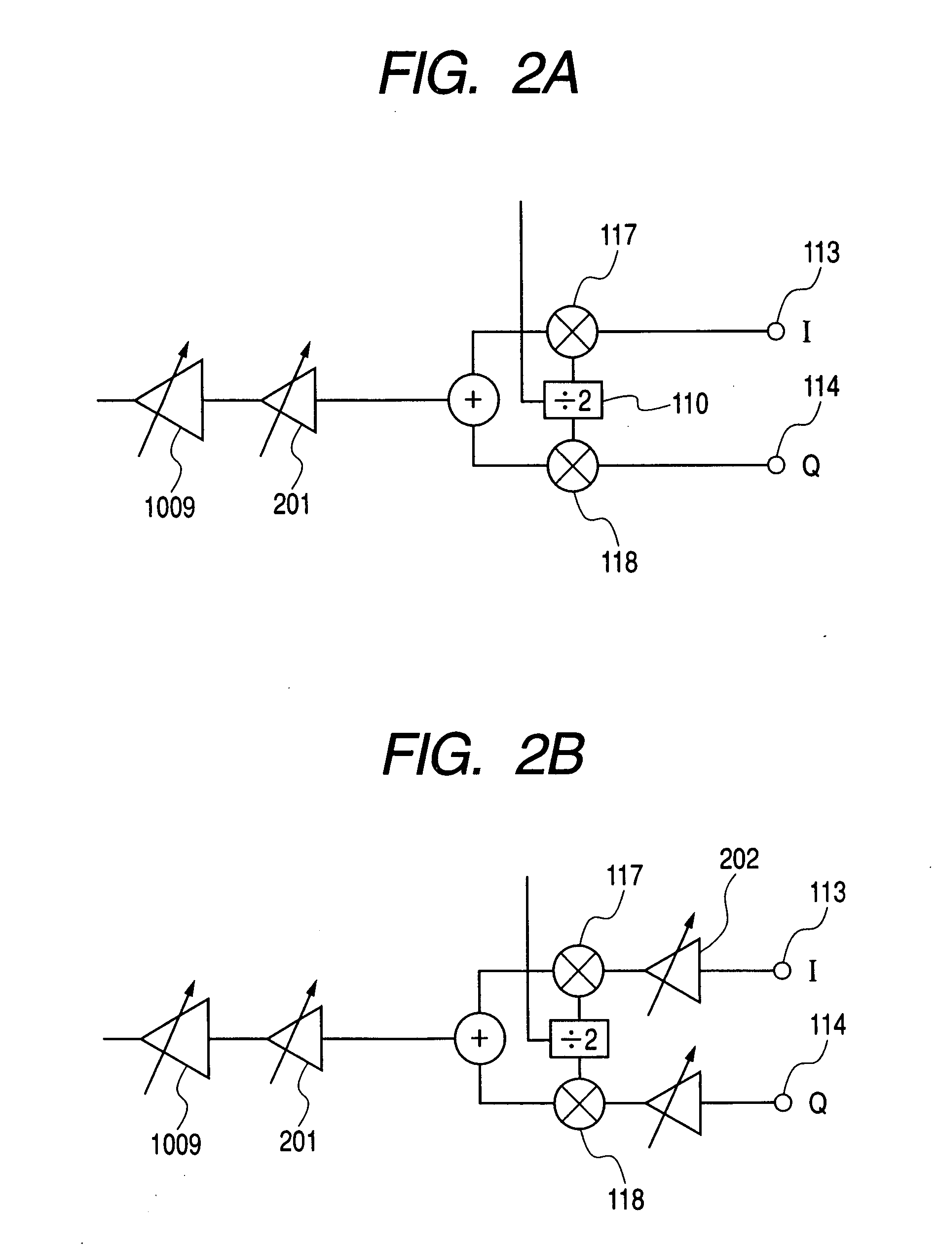
[0037]FIG. 2A is a view showing an example of circuit configuration when variable gain is realized by an orthogonal modulator having fixed gain and a high-frequency variable gain amplifier (RFGCA). The orthogonal modulator is composed of two mixers 117 and 118, and a divider 110 for generating two local oscillation signals having a 90° phase difference. To an I-signal input terminal 113 and a Q-signal input terminal 114, I-signal and Q-signal are applied respectively to convert into a high-frequency signal by the orthogonal modulator. The gain of the high-frequency signal converted is adjusted by a high-frequency variable gain amplifier 201.

[0038] The W-CDMA requests variable width of a signal level of 70 dB or high...

second embodiment

[0047] With reference to FIG. 5 to FIGS. 7A and 7B, the description will be made of a second embodiment according to the present invention. Although the current source which interlocks with the variable attenuator has been used in the first embodiment, in the present embodiment, bias of the mixer will be controlled by means of common mode DC voltage of the variable attenuator.

[0048]FIG. 5 shows circuit configuration of the present embodiment. Since I, Q both systems have the same configuration, detailed circuit configuration only concerning the I-system will be shown and the circuit configuration of the Q-system will be omitted hereinafter.

[0049] As in the case of the first embodiment, for the mixer 117, a Gilbert type mixer is applied, and the mixer 117 is driven by a secondary active filter circuit 501 for reducing an out-band noise level. The active filter circuit 501 is driven by a variable attenuator 502. The variable attenuator 502 attenuates a signal level, and also changes...

third embodiment

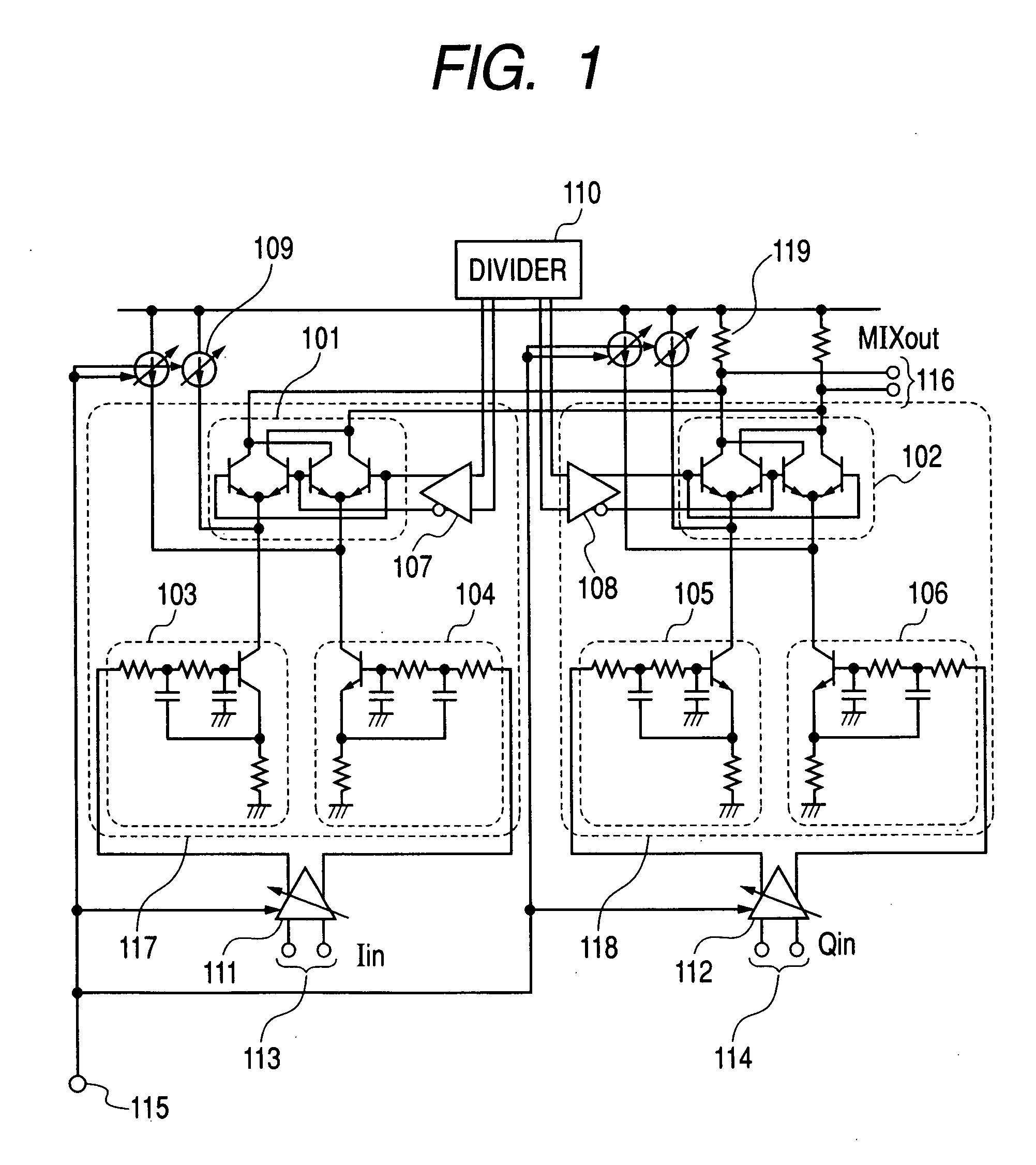
[0054] With reference to FIG. 8, the description will be made of a third embodiment of the present invention. In the present embodiment, mixers responsive to the signal level are connected in parallel, and are used by switching in accordance with the signal level, whereby it is possible to cope with reduction in carrier leak. FIG. 8 shows when two mixers 801 and 802 are connected in parallel. The mixer 801 is a high gain circuit, while the mixer 802 is a low gain circuit. The mixers 801 and 802 are constituted with size of transistor for constituting the circuit as n:1, and resistance as 1:n, and are set such that the driving current becomes n:1 at the same bias voltage. Even buffer circuits 803 and 804 for driving two mixer circuits are realized with similar transistor size ratio and resistance ratio.

[0055] These two mixers 801 and 802 are selected by an input circuit 809 at the previous stage. The input circuit is constituted by a plurality of selection circuits, each being compo...


PUM


Abstract

Disclosed is a direct conversion type transmitter or transceiver circuit suitable for a mobile communication device which corresponds to broad signal output level variable width to be required by W-CDMA, which does not necessitate any high-performance low noise VCO and RF filter, capable of reducing a number of components and the cost. In the input portion of an orthogonal modulator composed of a divider, mixers, and a common load, there are provided variable attenuators. If an input signal level of the orthogonal modulator within the transmitter circuit lowers, this variable attenuator circuit is operated so as to lower the bias of the orthogonal modulator to reduce the amount of occurrence of carrier leak, and to prevent the signal during low output level and carrier leak ratio from being deteriorated. The direct conversion transmitter circuit is capable of easily realizing output level variable width of 70 dB or higher and reducing a variable amount in the high frequency circuit in which it is difficult to secure the variable gain width.

Description

CROSS REFERENCE TO RELATED APPLICATIONS [0001] This application is a Divisional application of U.S. application Ser. No. 10 / 739,282 filed on Dec. 19, 2003. Priority is claimed based on U.S. application Ser. No. 10 / 739,282 filed on Dec. 19, 2003, which claims priority to Japanese Patent Application No. 2002-369761 filed on Dec. 20, 2002, all of which is incorporated by reference.FIELD OF THE INVENTION [0002] The present invention relates to a transmitter circuit and a transceiver system, and more particularly to a transmitter circuit suitable for a mobile communication device to which a direct conversion system suitable for large scale integration has been applied, and a transceiver system using the same. BACKGROUND OF THE INVENTION [0003] Along with the burst of penetration of the mobile communication devices, the request for miniaturization at lower cost has been increasing. For this reason, it is desired to apply an integrated circuit the integration density of which has been impr...

Claims


Application Information

Patent Timeline
Patent Type & Authority Applications(United States)
IPC IPC(8): H04B1/44H04M1/00H03C3/40H03D3/00H04B1/04H04B1/30H04B1/3822H04B1/40
CPCH03C3/40H03D3/007H04B1/30
Inventor TANAKA, SATOSHIYAMAWAKI, TAIZOHORI, KAZUAKIWATANABE, KAZUO
Owner RENESAS ELECTRONICS CORP
Why Eureka
Try Eureka