

Floating gate of flash memory device and method of forming the same
- Summary
- Abstract
- Description
- Claims
- Application Information
AI Technical Summary
Benefits of technology
Problems solved by technology
Method used
Image

Examples
Embodiment Construction
[0022] Hereinafter, a floating gate of a flash memory device and a method of forming the same according to the present invention will be described in detail with reference to the accompanying drawings.
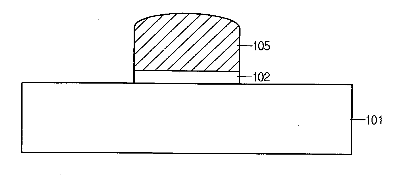
[0023]FIG. 1 is a sectional view showing a floating gate of a flash memory device according to the present invention.
[0024] As shown in FIG. 1, a tunneling oxide layer 102 is formed on a semiconductor substrate 101, and a floating gate is formed in the shape of a lens having a convex top surface.
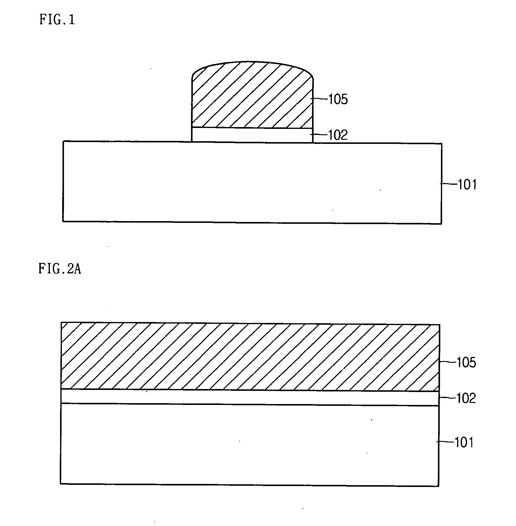
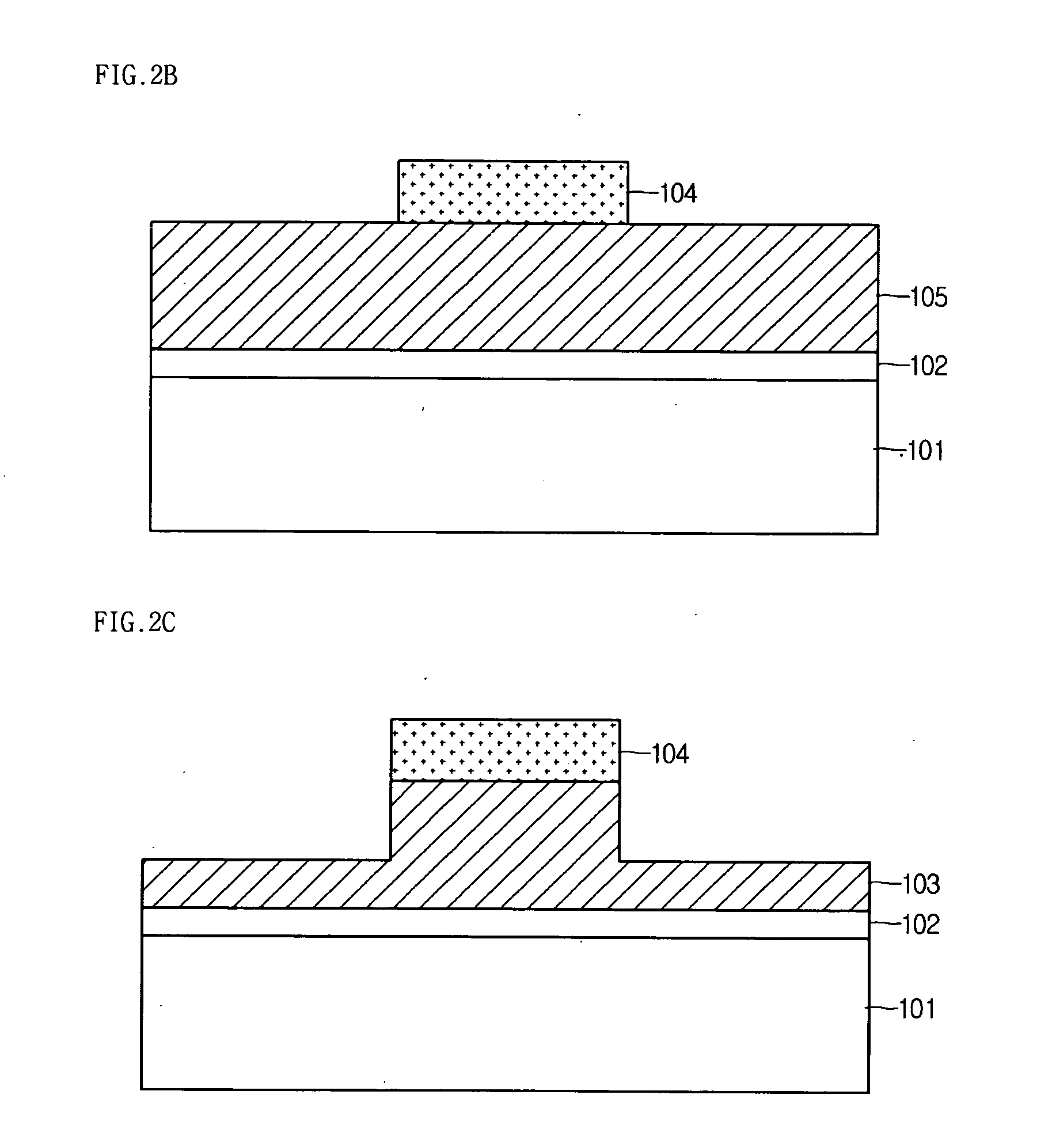
[0025]FIGS. 2A to 2E are sectional views illustrating a process of forming a floating gate in a flash memory device according to the present invention.
[0026] As shown in FIG. 2A, a tunneling oxide layer 102 is formed in a thickness of 80 to 120 Å on a semiconductor substrate 101, and a poly-silicon layer 103 is formed in a thickness of 900 to 1100 Å on the tunneling oxide layer 102.
[0027] Here, the poly-silicon 103 may be formed by allowing the thickness of the poly-silicon layer 103 to be...
PUM
 Abstract
Description
Claims
Application Information