EEPROM device for increasing a coupling ratio and fabrication method thereof

Inactive Publication Date: 2005-03-10
SAMSUNG ELECTRONICS CO LTD
View PDF8 Cites 7 Cited by
  • Summary
  • Abstract
  • Description
  • Claims
  • Application Information

AI Technical Summary

Benefits of technology

At least one embodiment of the present invention provides an Electrically Erasable and Programmable Read Only Memory (EEPROM) device capable of increasing a coupling ratio while overcoming the problems of the conventional EEPROM device.

Problems solved by technology

However, there is a limitation in lowering the thickness of the insulating layer 18 because it may result in charge loss.
Also, there is a limitation in reducing the size of the tunneling oxide layer 14 using a patterning process.
As a worst case scenario, a reduction in the size of the tunneling oxide layer 14 reduces the reliability of a memory device.

Method used


Image

  • EEPROM device for increasing a coupling ratio and fabrication method thereof
  • EEPROM device for increasing a coupling ratio and fabrication method thereof
  • EEPROM device for increasing a coupling ratio and fabrication method thereof

Examples


Embodiment Construction

The present invention will now be described more fully with reference to the accompanying drawings, in which example embodiments of the invention are shown. This invention may, however, be embodied in many different forms and should not be construed as being limited to the embodiments set forth herein. Rather, these embodiments are provided so that this disclosure will be thorough and complete and will fully convey the concept of the invention to those skilled in the art. Characteristics, such as shape and thickness, of elements shown in the drawings may be exaggerated for clarity. Or, in other words, the drawings are not drawn to scale. The same reference numerals represent the same elements throughout the drawings.

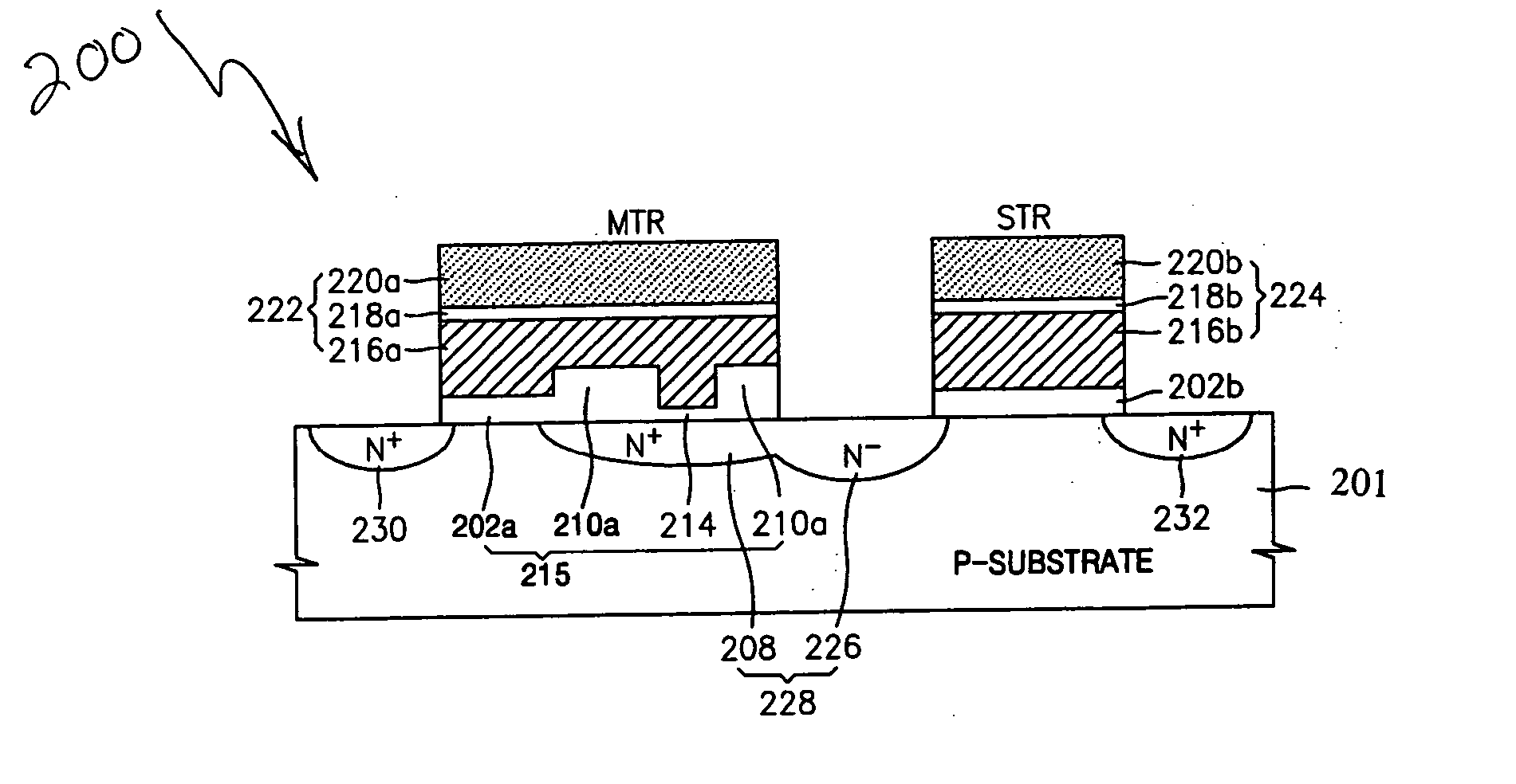
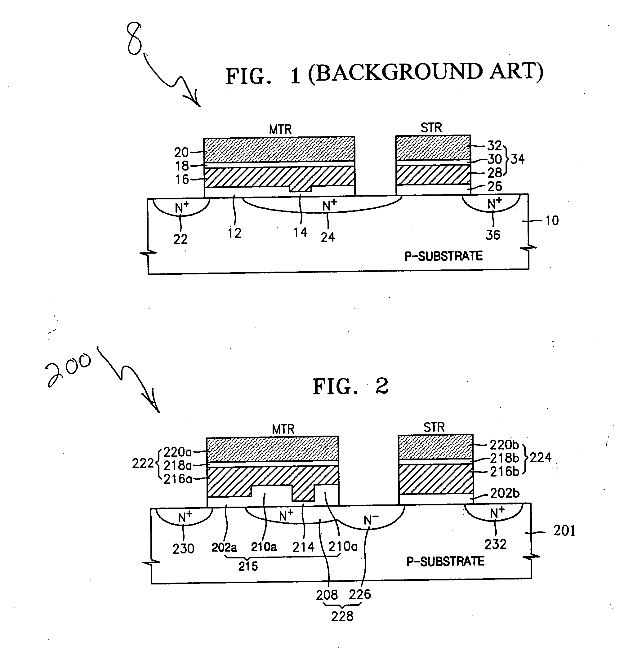
FIG. 2 is a cross-sectional view of a cell of an Electrically Erasable and Programmable Read Only Memory (EEPROM) device 200 according to at least one embodiment of the present invention.

More specifically, a memory transistor MTR and a selection transistor STR spaced...


PUM


Abstract

An electrically erasable and programmable read only memory (EEPROM) device may include: a gate oxide layer on a semiconductor substrate, the gate oxide layer including a first segment of a first thickness, a second segment of a second thickness, and a tunneling third segment of a third thickness, the second thickness being thicker than the first thickness and the third thickness being thinner than the first thickness; a floating junction region formed under a portion of the gate oxide layer in the semiconductor substrate; and a floating gate, an insulating layer pattern, and a control gate which are sequentially formed, respectively, on the gate oxide layer.

Description

This application claims the priorities of Korean Patent Application No. 2003-31910 filed on May 20, 2003, No. 2003-60763 filed on Sep. 1, 2003, and No. 2003-66943 filed on Sep. 26, 2003, the disclosures of which are incorporated herein in their entirety by reference. This application also is a continuation-in-part of copending U.S. patent application having Ser. No. 10 / 834,226 and Attorney Docket No. 2557-0000174 / US, filed Apr. 29, 2004, for which priority is claimed under 35 U.S.C. §120, and the disclosure of which is incorporated herein in its entirety. BACKGROUND OF THE INVENTION In general, there are various types of semiconductor memory devices such as Random Access Memory (RAM) and Read Only Memory (ROM). When power supply is disconnected, information stored in Random Access Memory (RAM) is lost, whereas information stored in Read Only Memory (ROM) is maintained. Therefore, the ROM is called a non-volatile memory device. An Electrically Erasable and Programmable Read Only M...

Claims


Application Information

Patent Timeline
IPC IPC(8): H01L21/28H01L21/336H01L21/8247H01L27/115H01L29/423H01L29/788
CPCH01L21/28273H01L27/115H01L27/11521H01L29/7881H01L29/42324H01L29/66825H01L27/11524H01L29/40114H10B69/00H10B41/35H10B41/30
Inventor KANG, SUNG-TAEGKIM, SEONG-GYUN
Owner SAMSUNG ELECTRONICS CO LTD
Why Eureka
Try Eureka