

Non-volatile memory with improved coupling rate and its making method
A non-volatile storage and conductive layer technology, applied in semiconductor/solid-state device manufacturing, electrical components, electric solid-state devices, etc., can solve the problems of reducing the dielectric layer, difficult charge pump design, increasing internal polysilicon, etc.
- Summary
- Abstract
- Description
- Claims
- Application Information
AI Technical Summary
Problems solved by technology
Method used
Image

Examples
Embodiment Construction
[0027] The present invention is described below with an example of a non-volatile semiconductor memory device. It should be understood, however, that the present invention is not limited to the use of a particular type of device or memory cell, and that the present invention is more broadly applicable to any semiconductor device in which internal impedance is a concern. Furthermore, while the present invention is well suited for use in non-volatile semiconductor memory devices, it also provides significant advantages in numerous other applications.
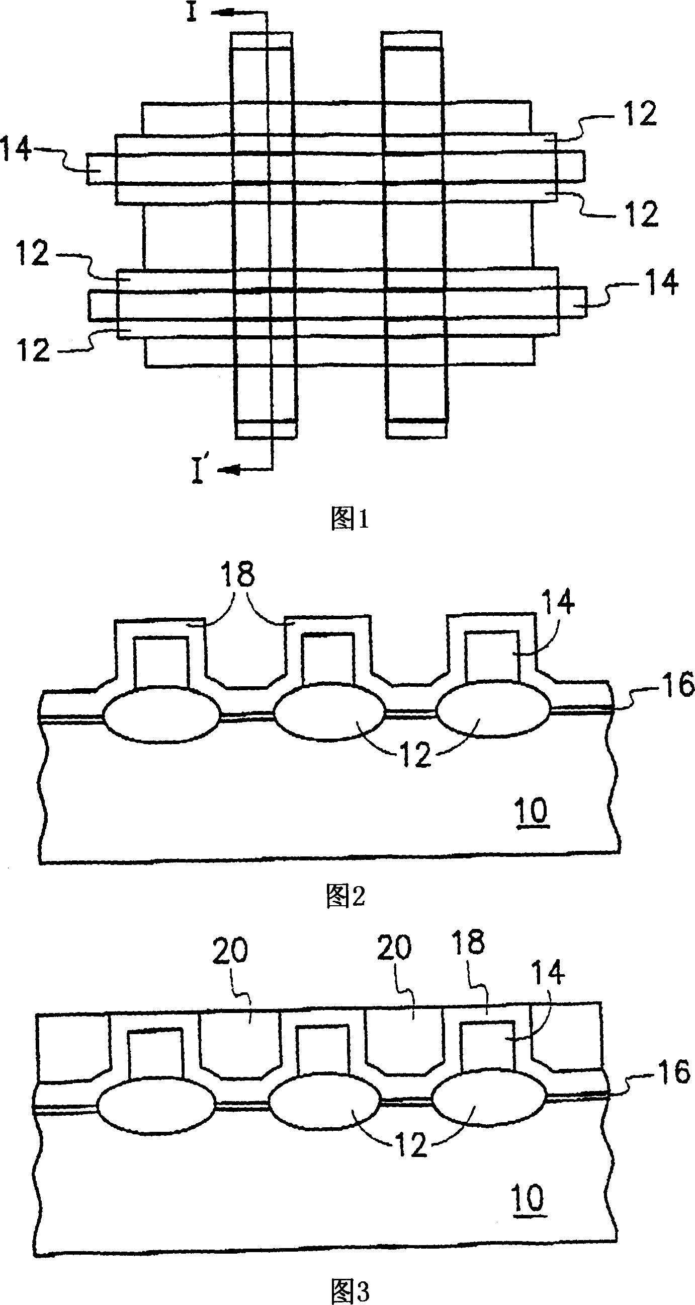
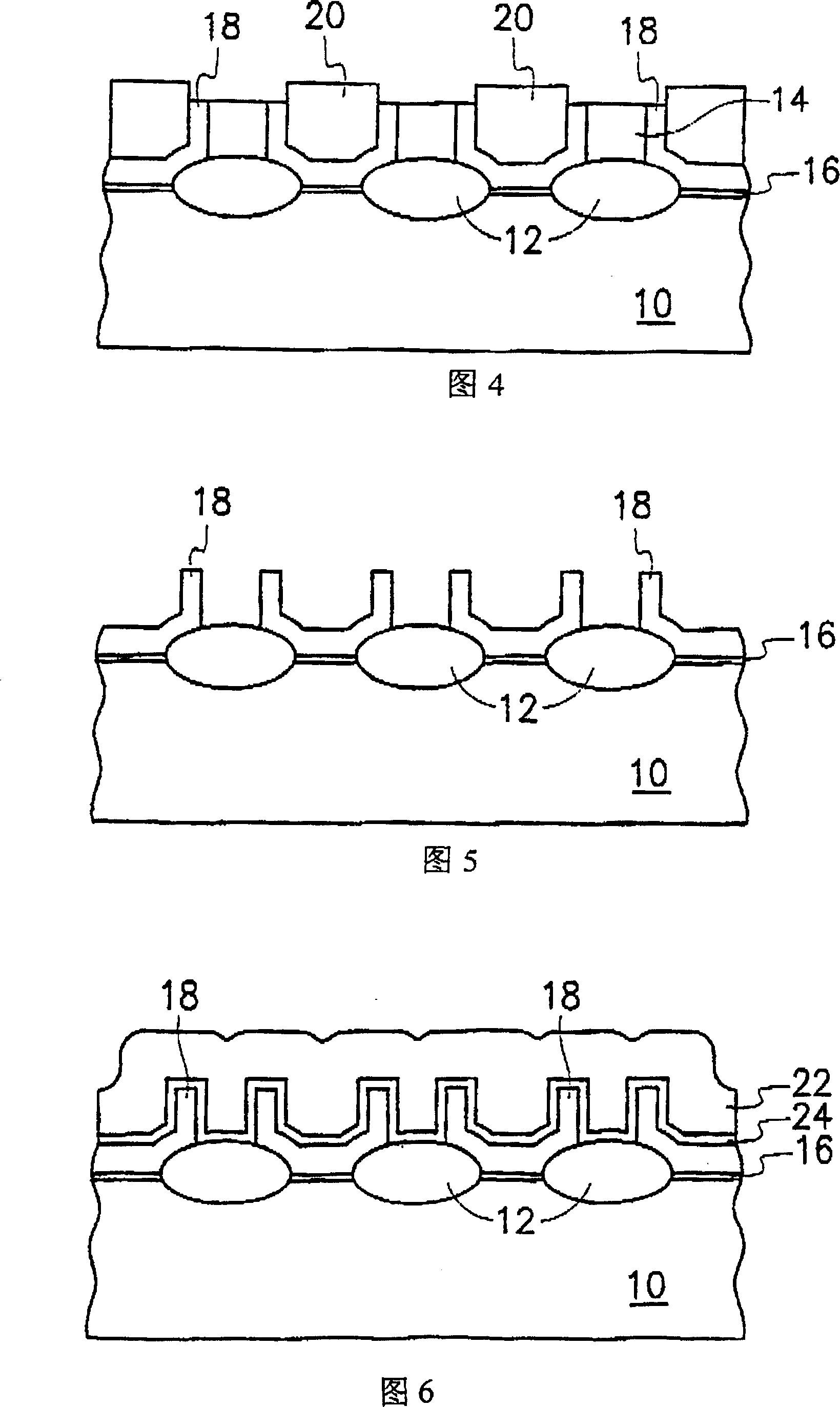
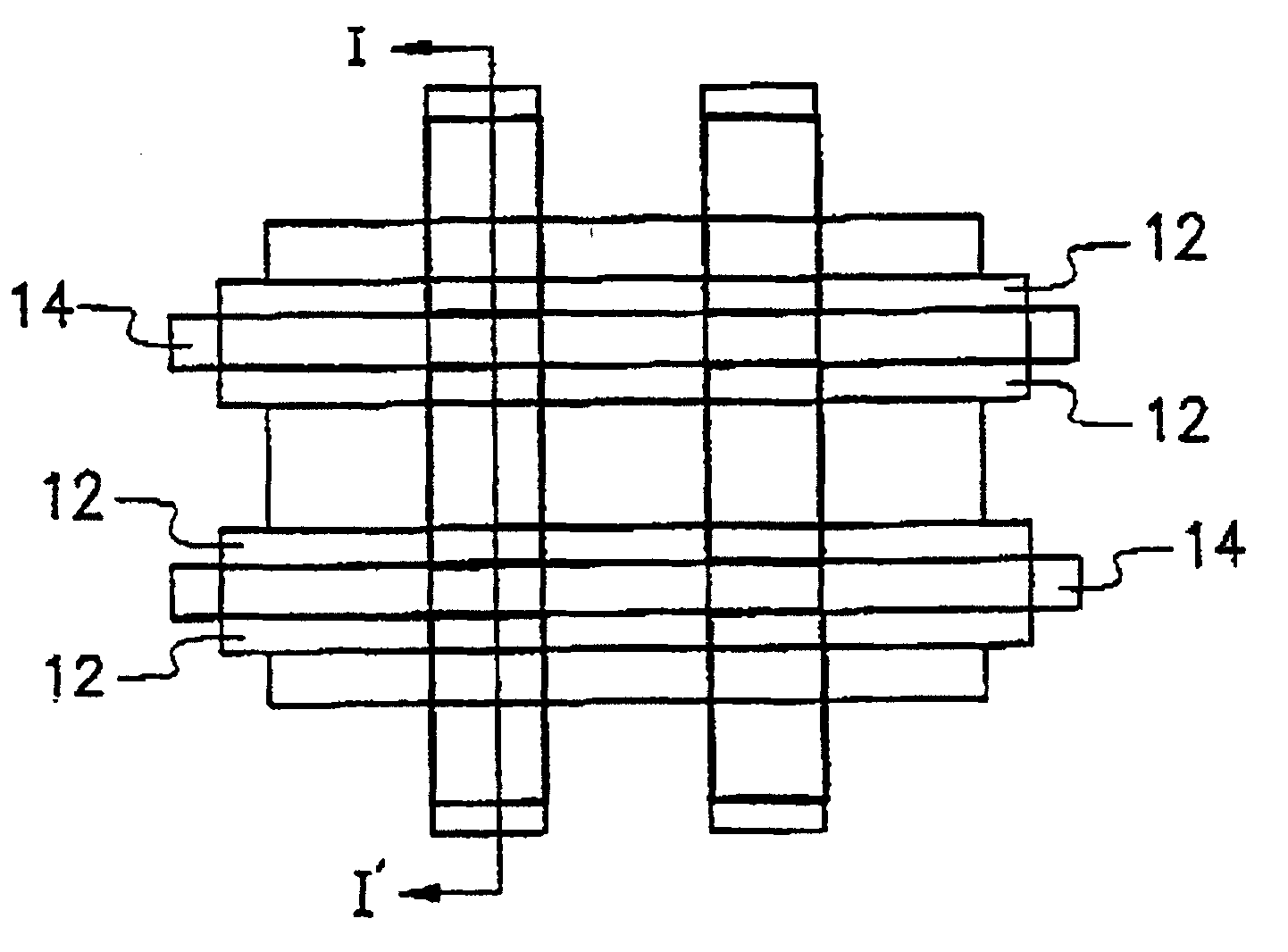
[0028] 1 to 6 show the process of forming an embodiment of the present invention, please refer to FIG. 1 and FIG. 2 (FIG. 2 is a cross-sectional view along the I'-I plane of FIG. As a starting point, a long line of an isolation region 12 is formed in the silicon substrate 10 by, for example, an area oxidation method, a first dielectric layer (for example, silicon nitride) 14 is formed on the isolation region 12 and the silicon sub...
PUM
 Abstract
Description
Claims
Application Information