
Flash memory structure and method of making the same

Inactive Publication Date: 2008-12-25
NAN YA TECH
View PDF4 Cites 4 Cited by
  • Summary
  • Abstract
  • Description
  • Claims
  • Application Information

AI Technical Summary

Benefits of technology

[0008]It is one objective of the present invention to provide an improved flash memory cell structure and fabrication method thereof. The present invention method is characterized in that the floating gate is formed prior to the formation of the control gate. By doing this, the coupling ratio between the floating gate and the control gate is increased. The present invention memory cell structure and its fabrication method are provided to reduce the alignment difficulty during the fabrication of the memory cell. Further, the present invention aims to solve the short channel effect.

Problems solved by technology

One major drawback of the above-described flash memory cell unit is its poor data retention capability.
Besides, as the size of the cells shrink, short channel effect and alignment become major problems to the manufacturers.

Method used


Image

  • Flash memory structure and method of making the same
  • Flash memory structure and method of making the same
  • Flash memory structure and method of making the same

Examples


Embodiment Construction

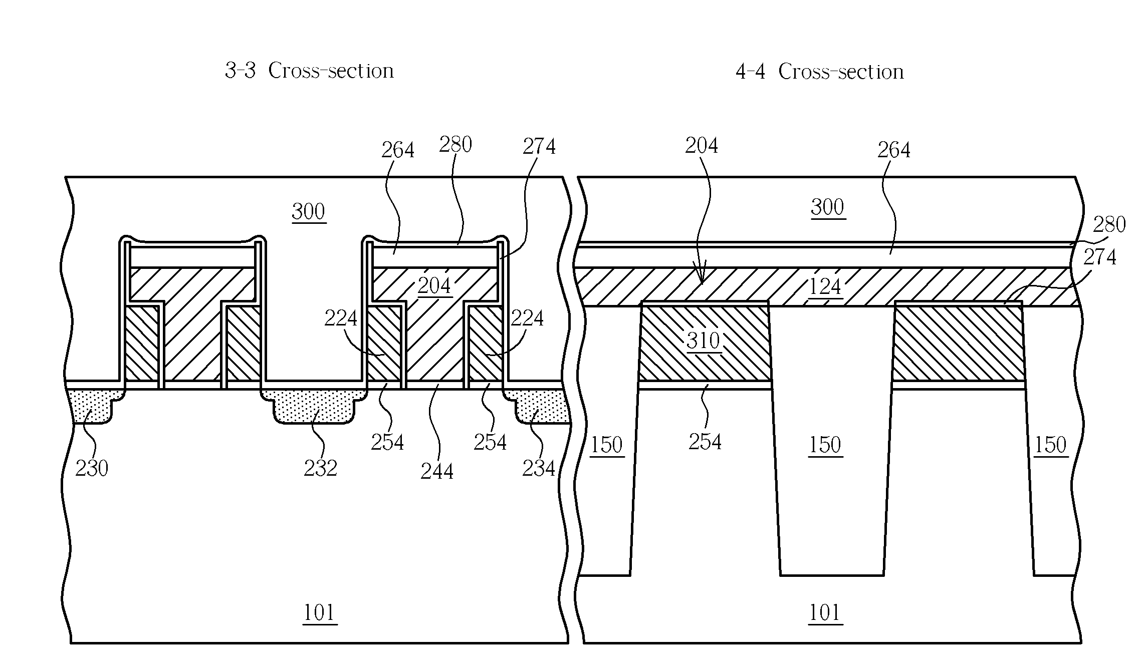
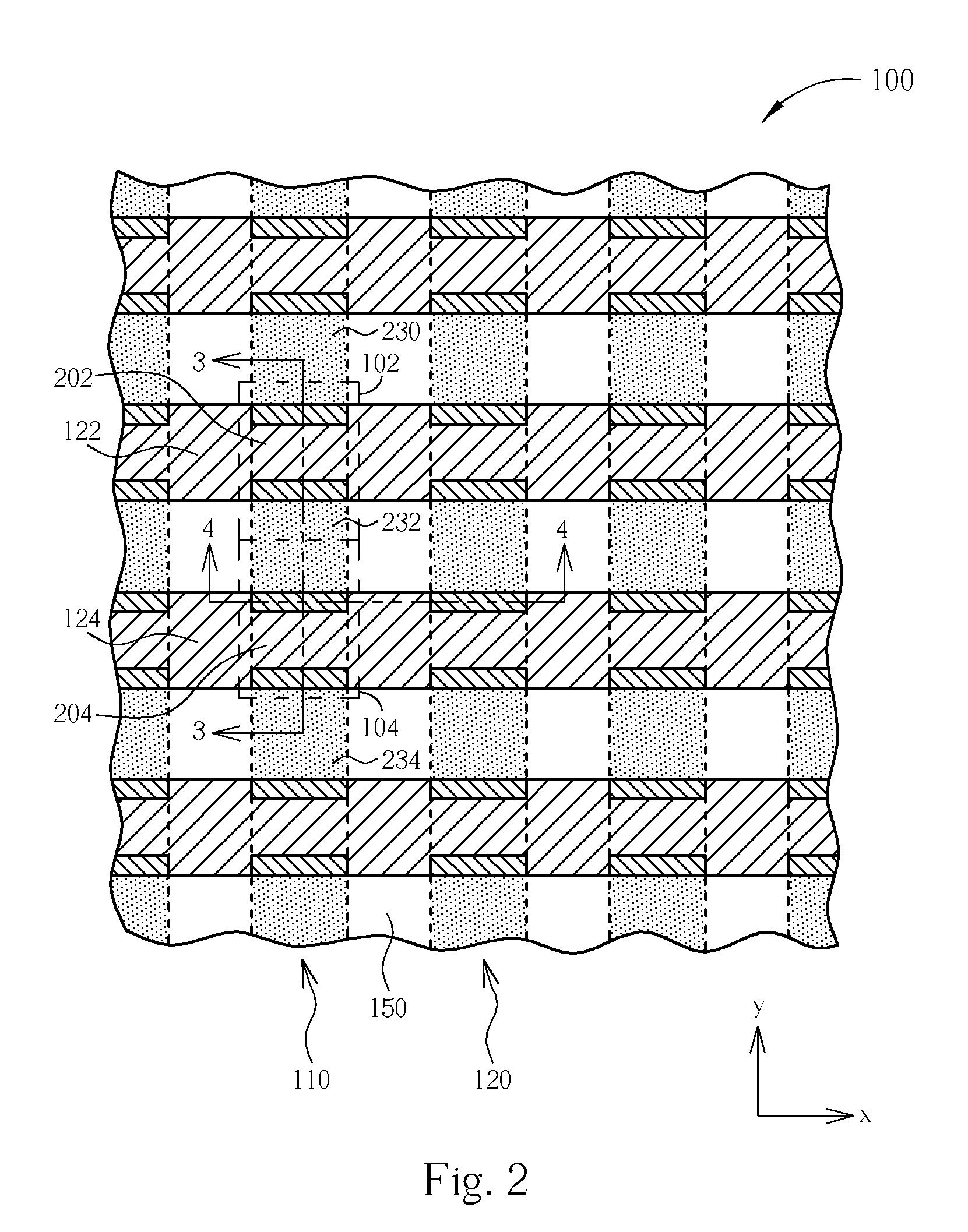
[0016]With reference to FIGS. 2 to 4, wherein FIG. 2 is a schematic layout view of an array of flash memory cells in accordance with the preferred embodiment of this invention, FIG. 3 is a schematic, cross-sectional view illustrating two adjacent flash memory cell units taken along line 3-3 of FIG. 2, and FIG. 4 is a cross-sectional diagram taken along line 4-4 of FIG. 2.

[0017]As shown in FIG. 2, the flash memory array 100 comprises a flash memory cell unit 102 and a flash memory cell unit 104 next to the flash memory cell unit 102. The flash memory cell unit 102 and the flash memory cell unit 104 are serially connected to one another along y-axis of a NAND memory block 110 and are part of a NAND memory block 110. The NAND memory block 110 may be a 16-bit memory block or 32-bit memory block, but not limited thereto.

[0018]The flash memory array 100 further comprises word line 122 and word line 124 disposed along the x-axis of the memory block 110. The word line 122 and word line 124 ...


PUM


Abstract

A flash memory cell includes a substrate, a T-shaped control gate disposed above the substrate, a floating gate embedded in a lower recess of the T-shaped control gate, a dielectric layer between the T-shaped control gate and the floating gate; a cap layer above the T-shaped control gate, a control gate oxide between the T-shaped control gate and the substrate, a floating gate oxide between the floating gate and the substrate, a liner covering the cap layer and the floating gate, and a source / drain region adjacent to the floating gate. The floating gate has a vertical wall surface that is coplanar with one side of the dielectric layer.

Description

BACKGROUND OF THE INVENTION [0001]1. Field of the Invention[0002]The present invention relates generally to the field of memory devices and fabrication method thereof. More particularly, the present invention relates to a flash memory cell structure with increased coupling ratio and method of making the same.[0003]2. Description of the Prior Art[0004]A flash memory is a non-volatile computer memory that can be electrically erased and reprogrammed. It is a technology that is primarily used in, for example, memory cards or USB flash drives, which are used for general storage and transfer of data between processors and other digital products. Presently, scaling down of flash memory cells has been considered critical in continuing the trend toward high device density.[0005]FIG. 1 is a schematic cross-sectional view showing a conventional two-bit flash memory cell unit. The conventional two-bit flash memory cell unit comprises a substrate 10, a composite dielectric layer 12 consisting of...

Claims


Application Information

Patent Timeline
IPC IPC(8): H01L29/00H01L21/336
CPCH01L27/115H01L27/11526H01L27/11543H01L27/11568H10B69/00H10B41/48H10B41/40H10B43/30
Inventor HSIAO, CHING-NANHUANG, CHUNG-LINTSAI, CHEN-YULEE, CHUNG-YUAN
Owner NAN YA TECH
Learn More