Differential amplifier circuit operable with wide range of input voltages
a technology of input voltage and amplifier circuit, which is applied in the direction of electric/magnetic computing, fluid mattresses, instruments, etc., can solve the problem of loss of proper operation regardless of circuit configuration
- Summary
- Abstract
- Description
- Claims
- Application Information
AI Technical Summary
Benefits of technology
Problems solved by technology
Method used
Image

Examples
first embodiment
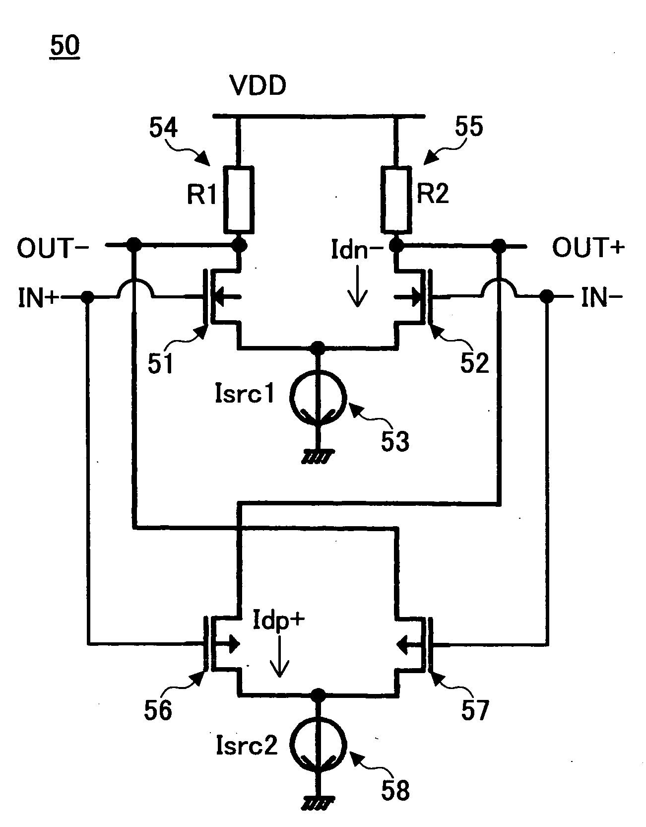
[0037]FIG. 4 is a drawing showing the circuit configuration of a differential amplifier circuit according to the present invention. A differential amplifier circuit 50 shown in FIG. 4 includes an NMOS transistor 51, an NMOS transistor 52, a constant current source 53, a resistor 54, a resistor 55, a PMOS transistor 56, a PMOS transistor 57, and a constant current source 58.
[0038] The resistor 54, the NMOS transistor 51, and the constant current source 53 are connected in series in the order named between the power supply voltage VDD and the ground voltage. Further, sharing the constant current source 53 with this series connection, the resistor 55, the NMOS transistor 52, and the constant current source 53 are connected in series in the order named between the power supply voltage VDD and the ground voltage.
[0039] The gate node of the NMOS transistor 51 serves as an input node IN+, and the gate node of the NMOS transistor 52 serves as an input node IN−. A joint point between the dr...
second embodiment
[0056]FIG. 6 is a drawing showing the circuit configuration of a differential amplifier circuit according to the present invention. A differential amplifier circuit 50A shown in FIG. 6 includes a PMOS transistor 101, a PMOS transistor 102, a constant current source 103, a resistor 104, a resistor 105, an NMOS transistor 106, an NMOS transistor 107, and a constant current source 108.
[0057] The resistor 104, the PMOS transistor 101, and the constant current source 103 are connected in series between the ground voltage and the power supply voltage VDD. Further, sharing the constant current source 103 with this series connection, the resistor 105, the PMOS transistor 102, and the constant current source 103 are connected in series between the ground voltage and the power supply voltage VDD.
[0058] The gate node of the PMOS transistor 101 serves as an input node IN+, and the gate node of the PMOS transistor 102 serves as an input node IN−. A joint point between the drain node of the PMOS...
third embodiment
[0063]FIG. 7 is a drawing showing the circuit configuration of a differential amplifier circuit according to the present invention. In FIG. 7, the same elements as those of FIG. 4 are referred to by the same numerals, and a description thereof will be omitted.
[0064] In a differential amplifier circuit 50B shown in FIG. 7, the resistors 54 and 55 of the differential amplifier circuit 50 shown in FIG. 4 are replaced with PMOS transistors 54A and 55A. Other parts of the configuration are the same between FIG. 7 and FIG. 4. The gate nodes of the PMOS transistors 54A and 55A receive a common bias voltage VBIAS.
[0065] Since the source-gate voltage of the PMOS transistors 54A and 55A is constant, the source-drain voltage can be changed significantly with little change in the drain currents Namely, the PMOS transistors 54A and 55A can serve as a resistor having an extremely large resistance. In the configuration shown in FIG. 7, the gate nodes of the PMOS transistors 54A and 55A receive th...
PUM
 Abstract
Description
Claims
Application Information
 - R&D
- Intellectual Property
- Life Sciences
- Materials
- Tech Scout
- Unparalleled Data Quality
- Higher Quality Content
- 60% Fewer Hallucinations
Browse by: Latest US Patents, China's latest patents, Technical Efficacy Thesaurus, Application Domain, Technology Topic, Popular Technical Reports.
© 2025 PatSnap. All rights reserved.Legal|Privacy policy|Modern Slavery Act Transparency Statement|Sitemap|About US| Contact US: help@patsnap.com