Semiconductor device and method of fabricating the same

Inactive Publication Date: 2007-06-28
KK TOSHIBA
View PDF4 Cites 33 Cited by
  • Summary
  • Abstract
  • Description
  • Claims
  • Application Information

AI Technical Summary

Problems solved by technology

When such the void is exposed to the surface of the semiconductor layer in the planarization step by CPM and results in a problem associated with mixture of dusts into the void, a problem arises because the delivery to the post step can not be achieved.

Method used


Image

  • Semiconductor device and method of fabricating the same
  • Semiconductor device and method of fabricating the same
  • Semiconductor device and method of fabricating the same

Examples


first embodiment

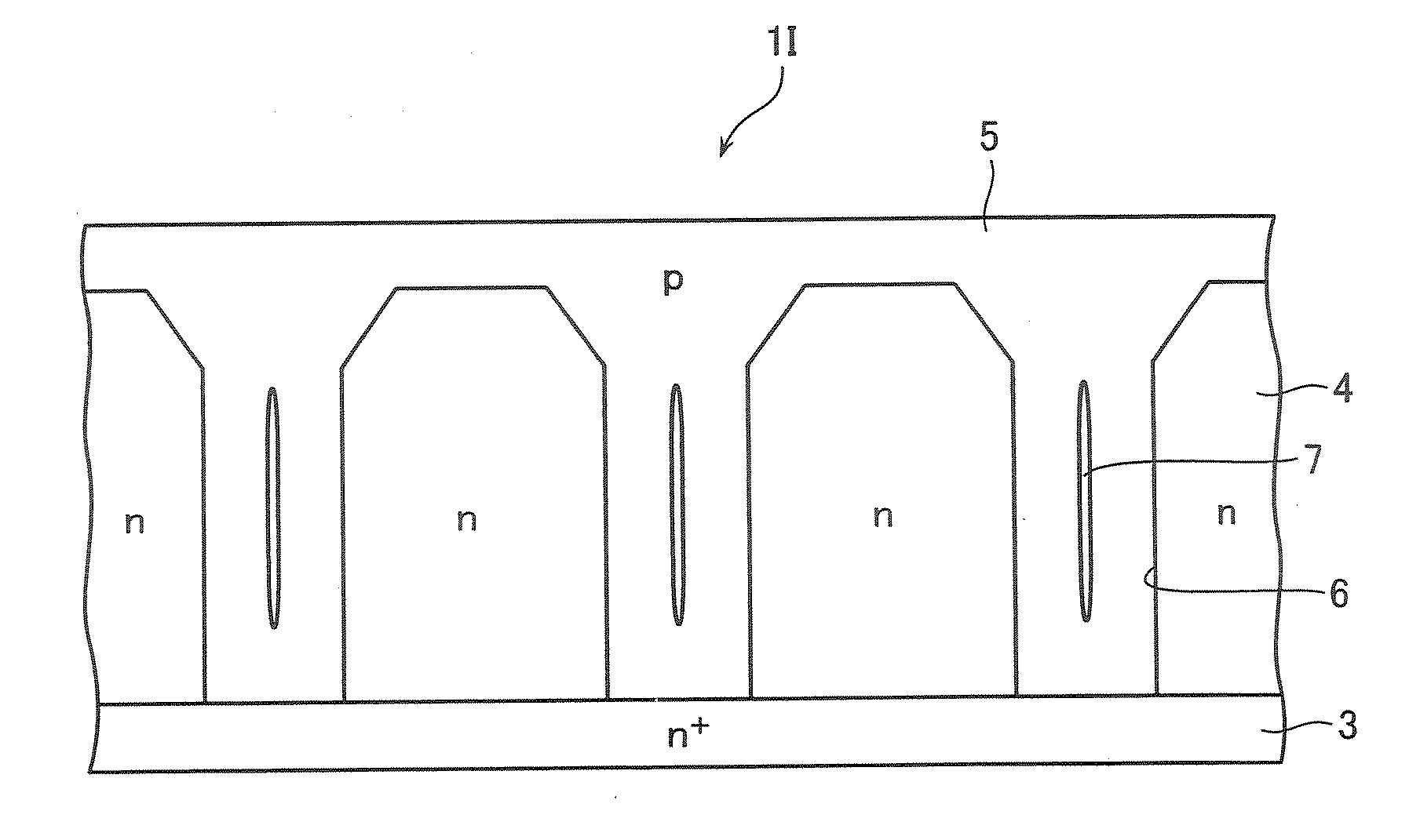
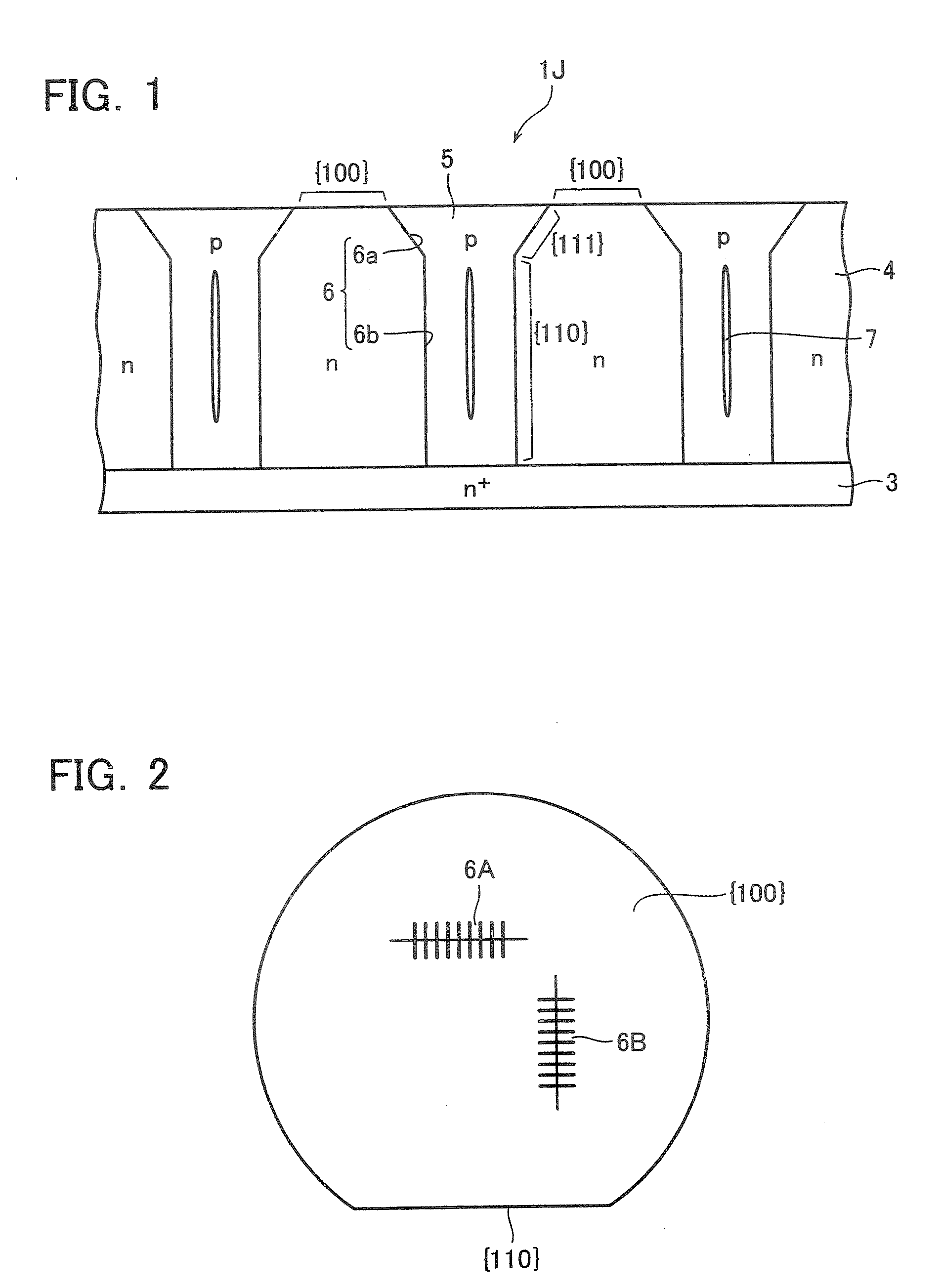
[0029]FIG. 1 is a partial vertical cross-sectional view of a semiconductor device, or an vertical SJ-MOSFET, during a fabrication process according to a first embodiment of the present invention. This semiconductor device 1J is configured as follows. An n+-type semiconductor substrate 3 (such as a silicon substrate) serves as a drain layer, on which an n-type first semiconductor layer 4 is disposed. A plurality of deep trenches 6 are formed periodically along the plane of the first semiconductor layer 4, and a p-type second semiconductor layer 5 is buried in the trenches 6 by epitaxial growth. A void 7 may possibly arise inside the second semiconductor layer 5 during the process of fabricating the semiconductor device 1J while this embodiment allows such the void to arise. The trench 6 is an elongated groove extending in the direction perpendicular to the page, or a groove having a square or rectangular lateral section. The trench 6 is defined by a V-grooved upper stage sidewall 6a ...

second embodiment

[0047]FIG. 16 is a vertical cross-sectional view showing a step during fabrication of a semiconductor device 1J′ according to a second embodiment of the present invention. In the semiconductor device 1J according to the first embodiment, the trenches 6 are formed such that the upper stage sidewall 6a has the surface orientation of substantially {111} and the lower stage sidewall 6b has the surface orientation of substantially {110}. To the contrary, in the second embodiment, trenches 6 are formed such that an upper stage sidewall 6a′ has a surface orientation of substantially {111} and a lower stage sidewall 6b′ has a surface orientation of substantially {100}. The growth speed of silicon in epitaxial growth varies in relation to {100}>{110}>>{111}. Accordingly, if the upper stage sidewall has the surface orientation of substantially {111}, the surface orientation of the lower stage sidewall may be either substantially {110} or substantially {100} to exert the above-described effect...

third embodiment

[0050]FIG. 18 is a vertical cross-sectional view of a semiconductor device according to a third embodiment. In the semiconductor device 1 of the first and second embodiments, the p-type base region 2 is formed deep such that a lower end thereof locates beneath the boundary between the upper stage sidewall 6a and the lower stage sidewall 6b of the trench 6. To the contrary, in the semiconductor device 1N of the third embodiment, the p-type base region 2 is formed such that a lower end thereof locates above a boundary 6Nc between an upper stage sidewall 6Na and a lower stage sidewall 6Nb of a trench 6N. Such the structure can exert the above-described effect.

[0051] In the above embodiments the present invention is applied to the power MOSFET having the superjunction structure including a plurality of deep trenches formed therein. The first through third embodiments can also be applied to any semiconductor devices that can be produced by forming trenches in the first semiconductor lay...


PUM


Abstract

The present invention provides a semiconductor device, which comprises a first semiconductor layer of the first conductivity type having a plurality of trenches formed therein. A second semiconductor layer of the second conductivity type composed of an epitaxial layer is buried in the trenches in the first semiconductor layer. The trench has surface orientations including a surface orientation of a sidewall at an upper stage made slower in epitaxial growth speed than a surface orientation of a sidewall at a lower stage.

Description

CROSS REFERENCE TO RELATED APPLICATION [0001] This application is based on and claims the benefit of prior Japanese Patent Application No. 2005-372739, filed on Dec. 26, 2005, the entire contents of which are incorporated herein by reference. BACKGROUND OF THE INVENTION [0002] 1. Field of the Invention [0003] The present invention relates to a semiconductor device, which has a structure that includes an epitaxial layer buried in trenches formed in a semiconductor layer, and method of fabricating the same. [0004] 2. Description of the Related Art [0005] In recent years, an SJ (Super Junction)-MOSFET has been known as one of low-loss power semiconductor devices. The SJ-MOSFET has a superjunction structure in a drift layer as a structure that satisfies a low on-resistance and a high breakdown voltage of a power MOSFET at the same time. In the SJ-MOSFET, trenches are formed in an n-type epitaxial layer periodically along the plane, and a p-type epitaxial layer is formed in these trenche...

Claims


Application Information

Patent Timeline
Patent Type & Authority Applications(United States)
IPC IPC(8): H01L21/336H01L21/461H01L21/22
CPCH01L29/045H01L29/0634H01L29/1095H01L29/66325H01L29/66712H01L29/7395H01L29/7802
Inventor TOKANO, KENICHISUGAYA, HIROYUKI
Owner KK TOSHIBA
Why Eureka
Try Eureka