Method and system of trace pull test

a pull test and trace pull technology, applied in the direction of individual semiconductor device testing, semiconductor/solid-state device testing/measurement, instruments, etc., can solve the problems of parts breaking within the package, and achieve the effect of determining the bonding quality of the package, easy upgrading the yield of the package, and testing the bonding quality of the di

Inactive Publication Date: 2007-07-05
ADVANCED CHIP ENG TECH INC
View PDF5 Cites 9 Cited by
  • Summary
  • Abstract
  • Description
  • Claims
  • Application Information

AI Technical Summary

Benefits of technology

[0008] The present invention fills the needs by providing a method and a system to test the bonding quality of dies. It should be appreciated that the present invention can be implemented in numerous ways, including as a process, a system, or a method. By using the method and system of the present invention, the manufacturer of package can truly find out the critical part of testing. Moreover, the manufacturer also can easily upgrade the yield of the package.
[0009] The purpose of the present invention is to determine the bonding quality of the package by measuring the strength which the bonding part can stand. By connecting the biases to conductive parts of the package, there will form a circuit loop. Then we apply an external force on bonding balls in vertical direction, and monitor the status of the circuit loop. The bonding ball will be deformed due to the external force applies on them and this external force will be indicated to the bonding pads by the elastic trace material. Then it will cause the deformation of the bonding parts and also the status of the formed circuit loop. When this circuit loop is in a closed condition, it means that all the bonds are still connected to each other. When this circuit loop is in an open condition, means that there are some parts broken within the package. At the same time, watching the difference of the external force, this can help the manufacture to determine the bonding quality of the package. Because the circuit loop is very sensitive, so we can consider the circuit loop as a trigger standing for the bonds breaking moment. By this circuit loop, we can exactly measure the bonding strength which the package can withhold.
[0010] Another purpose of the present invention is to determine the bonding quality of the package by measuring a dimension parameter of the bonding balls. By connecting the biases to bumps (conductive parts) of the package, there will form a circuit loop. Then we apply an external force on bonding balls in vertical direction, and monitor the dimension parameter of the deforming bonding balls. The bonding balls will be deformed because the external force applies on it and the elastic material forms the trace layer. Then it will cause the deformation of the bonding parts and also the status of the formed circuit loop. When this circuit loop is in a closed condition, it means that all the bonds are still connected to each other. Conversely, when this circuit loop is in an open condition, means that there are some parts broken within the package. At the meantime, pay attention to the dimension parameter in bonding balls. This can ensure whether the bonding quality of the package is superb or not. By referring to this measurement on the dimension parameter, the manufacturer also can improve the yield of their packaging process.

Problems solved by technology

Conversely, when this circuit loop is in an open condition, means that there are some parts broken within the package.

Method used


Image

  • Method and system of trace pull test
  • Method and system of trace pull test
  • Method and system of trace pull test

Examples


Embodiment Construction

[0016] The present invention is described with preferred embodiments and accompanying drawings. It should be appreciated that all the embodiments are merely used for illustration. Although the present invention has been described in term of a preferred embodiment, the invention is not limited to this embodiment. It will be understood, however, to one skilled in the art, that the present invention may be practiced without some or all of these specific details. In other instances, well known process operations have not been described in detail in order not to unnecessary obscure the present invention.

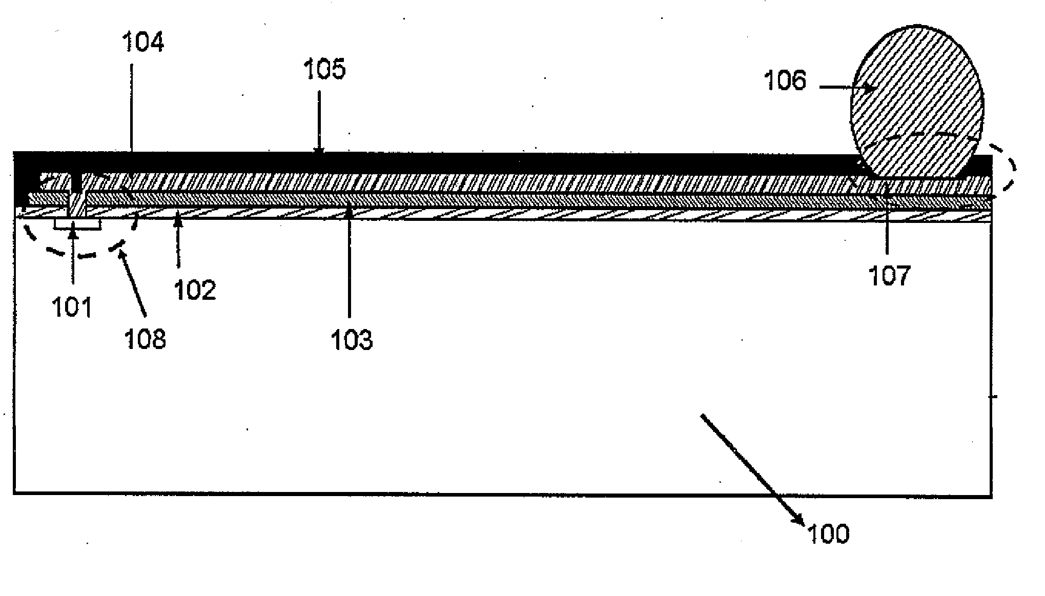
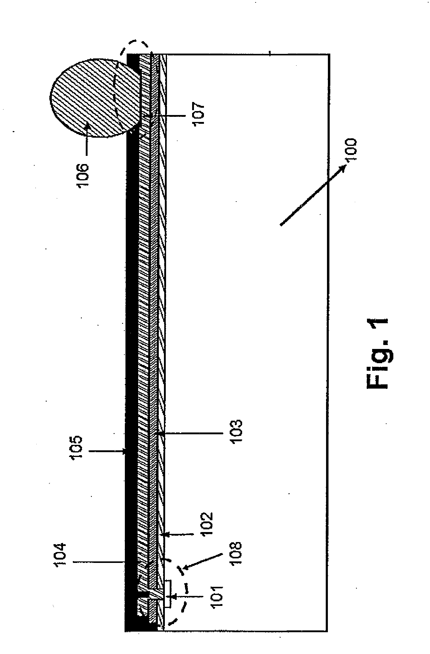
[0017] A partial package structure using in one of the preferred embodiment of the present invention is shown as FIG. 1. The package structure comprises an isolation layer 103 and a passivation layer 102 of an IC (integrated circuit) device 100. The material of the isolation layer 103 may be a dielectric layer with a thickness of 5 micron such as BCB, SINR (Siloxane polymer), epoxy, poly...


PUM

PropertyMeasurementUnit
thicknessaaaaaaaaaa
thicknessaaaaaaaaaa
force/lengthaaaaaaaaaa

Abstract

The present invention provides an efficient test method and system for testing the IC package, such as BGA types of packages. With the present invention, manufacturer can have an easier way in testing various types of packages, including newer types. Manufacturer also can get the testing outcome which is more accurate. Furthermore, help the manufacturer to achieve a quite improvement in IC packaging process.

Description

RELATED APPLICATIONS [0001] This application is a divisional of U.S. application Ser. No. 11 / 235,485, filed Sep. 26, 2005.FIELD OF THE INVENTION [0002] This invention relates to a method and system for testing the bonding strength and quality of packaged IC (integrated circuit), and more particularly to a novel method and system for testing the bonding strength and quality of wafer-level packaged IC (integrated circuit). BACKGROUND OF THE INVENTION [0003] The semiconductor technologies are developing very fast, especially for semiconductor dies which have a tendency toward miniaturization. Besides, the requirements for the functions of the semiconductor dies have an opposite tendency to variety. Namely, the semiconductor dies must have more I / O pads into a smaller area, so the density of the pins is raised quickly. It causes the packaging for the semiconductor dies to become more difficult and decrease the yield. [0004] The main purpose of the package structure is to protect the die...

Claims


Application Information

Patent Timeline
Patent Type & Authority Applications(United States)
IPC IPC(8): G01R31/02H01L21/66G01N3/00
CPCG01R1/07314H01L24/05H01L24/13H01L2224/05001H01L2224/05022H01L2224/05024H01L2224/05124H01L2224/05548H01L2224/11H01L2224/13024H01L2924/00014G01N3/00H01L22/00
Inventor YANG, WEN-KUNTAI, CHENG CHIEH
Owner ADVANCED CHIP ENG TECH INC
Why Eureka
Try Eureka