Thin integrated circuit device packages for improved radio frequency performance

a technology of integrated circuit devices and radio frequency performance, which is applied in the direction of semiconductor devices, semiconductor/solid-state device details, electrical equipment, etc., can solve the problems of extremely limited number of inductors or other transmission line elements that can be incorporated into the finished semiconductor package, and the gross line pitch of the package is limited, so as to facilitate the formation of leads and transmission line elements, improve radio frequency performance, and less design flexibility

Inactive Publication Date: 2007-08-02
AMKOR TECH INC DW US
View PDF99 Cites 26 Cited by
  • Summary
  • Abstract
  • Description
  • Claims
  • Application Information

AI Technical Summary

Benefits of technology

[0007] In accordance with the present invention, there is provided a semiconductor package or RF module which is adapted to provide improved radio frequency performance through the integration of one or more transmission line elements. The semiconductor package of the present invention has a tape based construction, which allows for the implementation of the fine pitches and spaces needed to allow for the integration of one or more transmission line elements such as inductors, shortwave couplers, baluns and filters into the semiconductor package. In such tape based construction, metal layers are applied to each of the opposed sides or faces of a non-conductive film, with a subtractive or additive method thereafter being employed to facilitate the formation of leads and transmission line elements upon the film in any one of a variety of different configurations. Thus, the present invention represents a substantial departure from and provides significant advantages over leadframe based inductors for semiconductor packages which, due to their comparatively gross pitches and spaces, provide substantially less design flexibility.

Problems solved by technology

However, a major drawback associated with currently known leadframe based inductors for semiconductor packages such as RF modules is that such packages are limited to gross lines and pitches, typically on the order of six mil lines on six mil spaces.
As a result, the number of inductors or other transmission line elements that can be incorporated into the finished semiconductor package are extremely limited.

Method used


Image

  • Thin integrated circuit device packages for improved radio frequency performance
  • Thin integrated circuit device packages for improved radio frequency performance
  • Thin integrated circuit device packages for improved radio frequency performance

Examples


Embodiment Construction

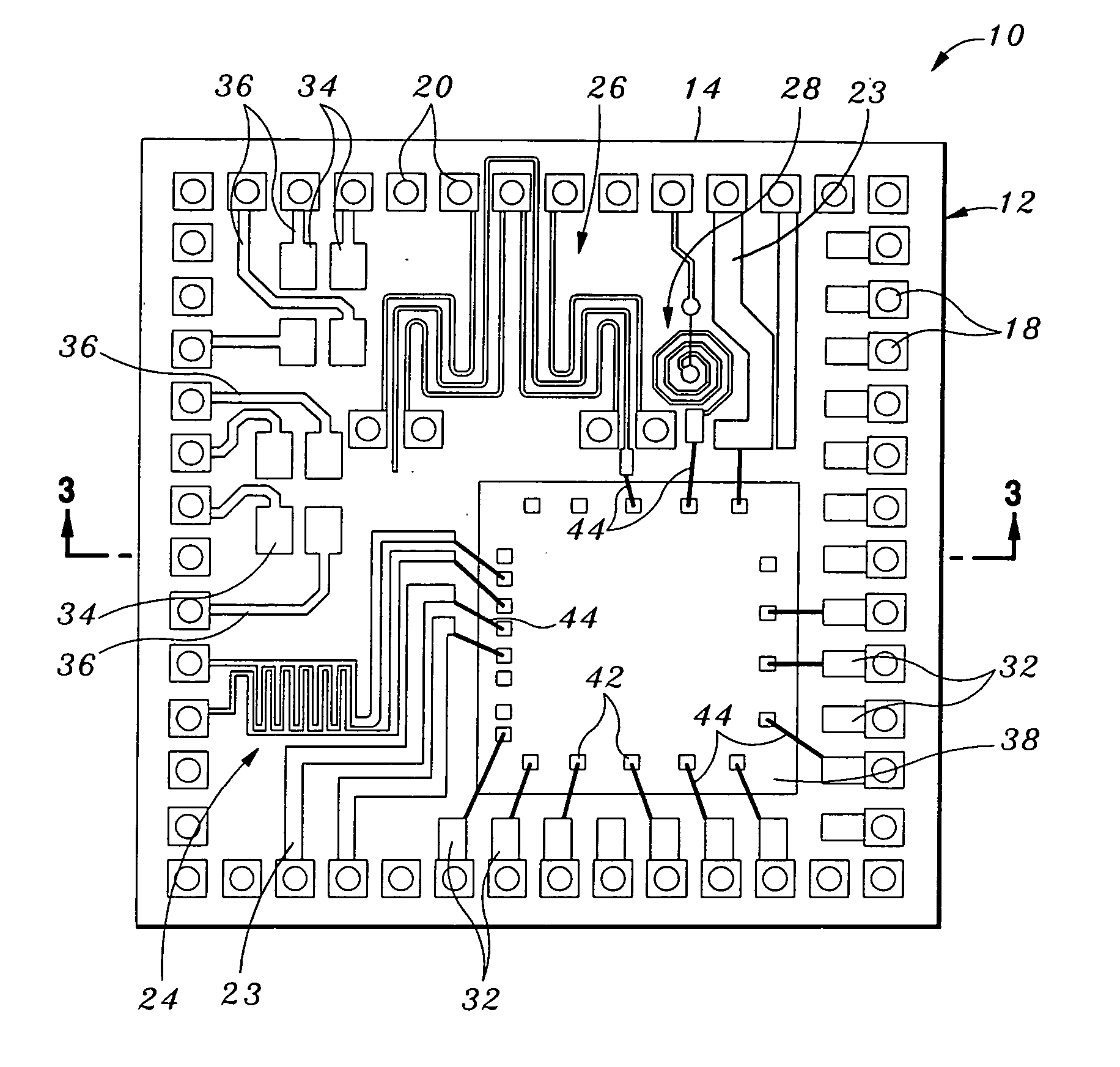
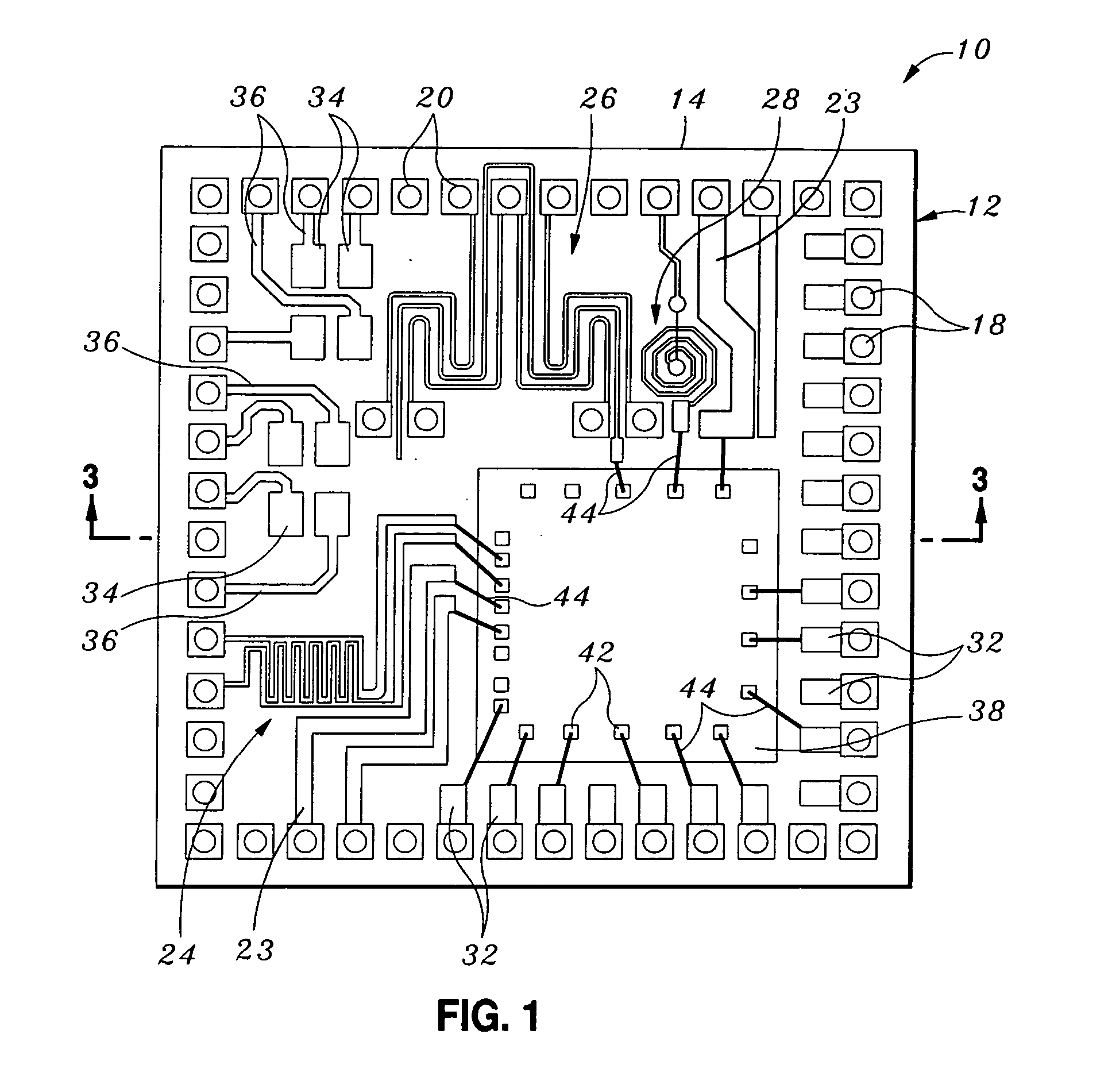
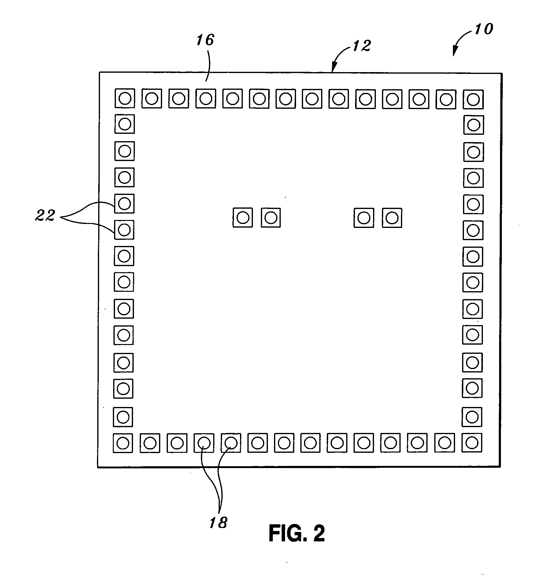
[0014] Referring now to the drawings wherein the showings are for purposes of illustrating a preferred embodiment of the present invention only, and not for purposes of limiting the same, FIGS. 1-3 depict a semiconductor package 10 constructed in accordance with the present invention. As will be described in more detail below, the semiconductor package 10 is outfitted with structural elements which make the same uniquely suited for use as a radio frequency (RF) module. However, those of ordinary skill in the art will recognize that the manufacturing methodology for the semiconductor package 10 which will be described in more detail below is also applicable to semiconductor packages having configurations adapted for use in applications other than as an RF module.

[0015] The semiconductor package 10 comprises a tape or film layer 12 which defines a generally planar top surface 14 and an opposed, generally planar bottom surface 16. In this regard, the film layer 12 is a generally plana...


PUM


Abstract

A semiconductor package comprising a non-conductive film which defines opposed top and bottom film surfaces and includes a plurality of vias disposed therein. Disposed on the top film surface is a plurality of upper leads which circumvent respective ones of the vias. Similarly, disposed on the bottom film surface is a plurality of lower leads which circumvent respective ones of the vias and are electrically connected to respective ones of the upper leads. At least one transmission line element is also disposed on the top film surface and electrically connected to at least one of the upper leads. Attached to the top film surface and electrically connected to at least one of the upper leads and the transmission line element is at least one semiconductor die. A package body at least partially covers the semiconductor die, the upper leads, the transmission line element, and the top film surface.

Description

CROSS-REFERENCE TO RELATED APPLICATIONS [0001] The present application is a continuation-in-part of U.S. application Ser. No. 10 / 667,759 entitled METHODS OF MAKING THIN INTEGRATED CIRCUIT DEVICE PACKAGES WITH IMPROVED THERMAL PERFORMANCE AND INCREASED I / O DENSITY filed Sep. 22, 2003, which is a continuation-in-part of U.S. application Ser. No. 10 / 354,772 entitled INTEGRATED CIRCUIT DEVICE PACKAGES AND SUBSTRATES FOR MAKING THE PACKAGES filed Jan. 30, 2003, which is a continuation of U.S. application Ser. No. 09 / 434,589 entitled INTEGRATED CIRCUIT DEVICE PACKAGES AND SUBSTRATES FOR MAKING THE PACKAGES filed Nov. 5, 1999 and issued as U.S. Pat. No. 6,580,159 on Jun. 17, 2003, the disclosures of which are incorporated herein by reference.STATEMENT RE: FEDERALLY SPONSORED RESEARCH / DEVELOPMENT [0002] Not Applicable BACKGROUND OF THE INVENTION [0003] The present invention relates generally to plastic semiconductor packages, and more particularly, to a semiconductor package adapted for imp...

Claims


Application Information

Patent Timeline
Patent Type & Authority Applications(United States)
IPC IPC(8): H01L23/34
CPCH01L23/3121H01L23/66H01L2224/48227H01L2224/32225H01L2924/01033H01L24/49H01L2924/3011H01L2924/30107H01L2924/19107H01L2924/19042H01L2924/19041H01L2924/19015H01L2924/14H01L2924/078H01L2924/01082H01L2924/01079H01L2924/01078H01L2924/01075H01L2924/01029H01L2924/01027H01L2924/01013H01L24/28H01L24/48H01L24/97H01L2224/16H01L2224/48091H01L2224/48195H01L2224/48228H01L2224/49171H01L2224/73265H01L2224/97H01L2924/00014H01L2924/00012H01L2924/00H01L2924/181H01L24/73H01L2224/05554H01L2224/45099H01L2224/45015H01L2924/207
Inventor CROWLEY, SEAN T.BANCOD, LUDOVICO E.DAVIS, TERRYDARVEAUX, ROBERT F.GAYNOR, MICHAEL P.
Owner AMKOR TECH INC DW US
Why Eureka
Try Eureka