Bipolar transistor with graded base layer

a base layer and bipolar transistor technology, applied in the direction of basic electric elements, electrical apparatus, semiconductor devices, etc., can solve the problems of conduction band spike at the emitter-base interface, limit the usefulness of devices for low power applications, etc., to reduce the injection of reverse holes, and improve the management of voltage budgets

Inactive Publication Date: 2005-06-30
IQE KC
View PDF14 Cites 21 Cited by
  • Summary
  • Abstract
  • Description
  • Claims
  • Application Information

AI Technical Summary

Benefits of technology

[0007] In one aspect, the HBT has a base layer comprised of a III-V material that includes indium and nitrogen. The III-V material of the base layer has a carbon dopant concentration of about 1.5×1019 cm−3 to about 7.0×1019 cm−3. In a preferred embodiment, the base layer includes the elements gallium, indium, arsenic, and nitrogen. The presence of indium and nitrogen reduces the band gap of the material relative to the band gap of GaAs. In addition, the dopant concentration in the material is high, the sheet resistivity (Rsb) is low. These factors result in a lower turn-on voltage relative to HBTs having a GaAs base layer with a similar dopant concentration.
[0029] The reduction in turn-on voltage can result in better management of the voltage budget on both wired and wireless GaAs-based RF circuits, which are constrained either by standard fixed voltage supplies or by battery output. Lowering the turn-on voltage can also alter the relative magnitude of the various base current components in a GaAs-based HBT. DC current gain stability as a function of both junction temperature and applied stress has been previously shown to rely critically on the relative magnitudes of the base current components. A reduction in reverse hole injection enabled by a low turn-on voltage is favorable for both the temperature stability and long-term reliability of the device. Thus, relatively strain-free Ga1-xInxAs1-yNy base materials having a high dopant concentration can significantly enhance RF performance in GaAs-based HBTs and DHBTs.

Problems solved by technology

The turn-on voltage can limit the usefulness of devices for low power applications in which supply voltages are constrained by battery technology and the power requirements of other components.
HBTs, however, can suffer from the disadvantage of having an abrupt discontinuity in the band alignment of the semiconductor material at the heterojunction can lead to a conduction band spike at the emitter-base interface of the HBT.

Method used


Image

  • Bipolar transistor with graded base layer
  • Bipolar transistor with graded base layer
  • Bipolar transistor with graded base layer

Examples


example 1

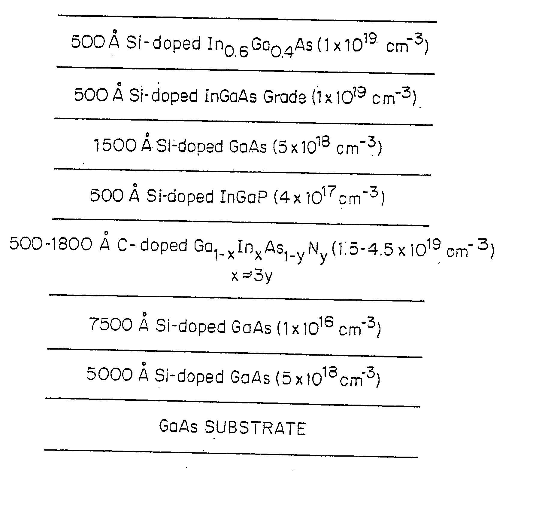
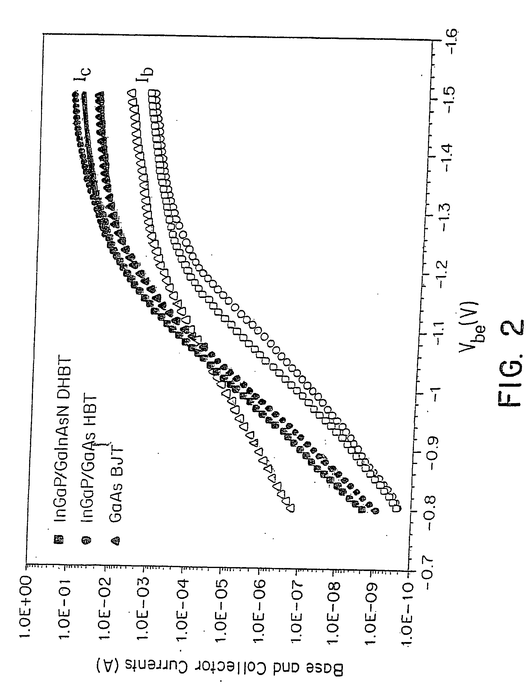
[0070] To illustrate the effect of reducing the band gap of the base layer and / or minimizing the conduction band spike at the emitter / base heterojunction, three different types of GaAs-based bipolar transistor structures were compared: GaAs emitter / GaAs base BJTs, InGaP / GaAs HBTs, and InGaP / GaInAsN DHBTs of the invention. A general representation of InGaP / GaInAsN DHBT structures used in the following experiments is illustrated in FIG. 1. There is only one heterojunction at the emitter / base interface since the base and the collector are both formed from GaAs. The GaAs base layer of the InGaP / GaAs HBT has a larger band gap than the base of the InGaP / GaInAsN DHBT. GaAs / GaAs BJTs have no heterojunctions since the emitter, collector and base are all made of GaAs. Thus, GaAs BJT structures are used as a reference to determine what impact, if any, a conduction band spike at the base-emitter interface has on the collector current characteristics of InGaP / GaAs HBTs. In the DHBTs of FIG. 1, I...

example 2

[0093] All of the GaAs devices used in the following discussion were MOCVD-grown, carbon-doped base layers in which the dopant concentration varied from about 3.0×1019 cm−3 to about 5.0×1019 cm−3 and a thickness which varied from about 500 Å to about 1500 Å, resulting in a base sheet resistivity (Rsb) of between 100 W / □ and 650 W / □. Large area devices (L=75 mm×75 mm) were fabricated using a simple wet-etching process and tested in the common base configuration. Relatively small amounts of indium (x˜1% to 6%) and nitrogen (y˜0.3%) were added incrementally to form two separate sets of InGaP / GaInAsN DHBTs. For each set, growth was optimized to maintain relatively high, uniform carbon dopant levels (>2.5×1019 cm−3), good mobility (˜85 cm2 / V-s), and high dc current gain (>60 at Rsb˜300 W / square). The structure of a DHBT used in the following experiments having a compositionally graded GaInAsN base layer is shown in FIG. 13. Alternative structures for DHBTs having compositionally garded b...

example 3

[0101] In order to improve the amplifier efficiency and thus lower the operating voltage and extend the battery lifetime, it is desirable to reduce the offset voltage (VCE,sat) and the knee voltage (Vk). One method of lowering the offset voltage is to minimize the asymmetry in turn-on voltages of the base / emitter and base / collector diode pair. DHBTs having wide bandgap collectors have been shown to yield low VCE,sat values, but in practice this leads to a higher Vk and reduces efficiencies because it is difficult to control the potential barrier at the base / collector heterojunction.

[0102] Insertion of a thin layer having a high bandgap (tunneling collector) allowed VCE,sat and Vk to be simultaneously reduced improving the efficiency of the device. FIG. 22 shows a schematic diagram of a DHBT that has a graded GaInAsN base layer and a tunneling collector. The base layer was graded such that there is about a 40 meV bandgap energy difference between the emitter and the collector juncti...


PUM

PropertyMeasurementUnit
band gapaaaaaaaaaa
band gapaaaaaaaaaa
band gapaaaaaaaaaa

Abstract

A semiconductor material which has a high carbon dopant concentration includes gallium, indium, arsenic and nitrogen. The disclosed semiconductor materials have a low sheet resistivity because of the high carbon dopant concentrations obtained. The material can be the base layer of gallium arsenide-based heterojunction bipolar transistors and can be lattice-matched to gallium arsenide emitter and / or collector layers by controlling concentrations of indium and nitrogen in the base layer. The base layer can have a graded band gap that is formed by changing the flow rates during deposition of III and V additive elements employed to reduce band gap relative to different III-V elements that represent the bulk of the layer. The flow rates of the III and V additive elements maintain an essentially constant doping-mobility product value during deposition and can be regulated to obtain pre-selected base-emitter voltages at junctions within a resulting transistor.

Description

RELATED APPLICATIONS [0001] This application is a continuation-in-part of U.S. application Ser. No. 10 / 121,444, filed Apr. 10, 2002, which is a continuation-in-part of U.S. application Ser. No. 09 / 995,079, filed Nov. 27, 2001, which claims the benefit of U.S. Provisional Application No. 60 / 253,159, filed Nov. 27, 2000, the teachings of all of which are incorporated herein in their entirety. U.S. application Ser. No. 10 / 121,444 also claims the benefit of U.S. Provisional Application No. 60 / 370,758, filed Apr. 5, 2002, and of U.S. Provisional Application No. 60 / 371,648, filed Apr. 10, 2002, the teachings of all of which are incorporated herein in their entirety.GOVERNMENT SUPPORT [0002] The invention was supported, in whole or in part, by a grant F33615-99-C-1510 from the Small Business Technology Transfer (STTR) Program of the United States Air Force. The Government has certain rights in the invention.BACKGROUND OF THE INVENTION [0003] Bipolar junction transistors (BJT) and heterojun...

Claims


Application Information

Patent Timeline
Patent Type & Authority Applications(United States)
IPC IPC(8): H01L21/331H01L29/10H01L29/20H01L29/737
CPCH01L29/1004H01L29/7371H01L29/66318H01L29/2003
Inventor WELSER, ROGER E.DELUCA, PAUL M.LUTZ, CHARLES R.STEVENS, KEVIN S.PAN, NOREN
Owner IQE KC
Why Eureka
Try Eureka