Semiconductor device

a technology of semiconductor devices and dielectric devices, which is applied in the direction of semiconductor devices, semiconductor/solid-state device details, electrical apparatus, etc., can solve the problems of reducing the mobility of the inversion layer, increasing the fixed electrical charge in the layer, and difficulty in maintaining the dielectric properties of high-k materials. , to achieve the effect of suppressing the increase of fn leakage current, high reliability, and high speed operation

Inactive Publication Date: 2005-03-10
HITACHI LTD
View PDF3 Cites 15 Cited by
  • Summary
  • Abstract
  • Description
  • Claims
  • Application Information

AI Technical Summary

Benefits of technology

[0031] According to the present invention, the gate insulating layer made of SiON is in the compressed strain state and the band gap of the gate insulating layer is larger as compared with the case of the strainless state or the tensile strain state, so that there can be provided the semiconductor device provided with the gate insulating layer structure having the satisfactory characteristics that the probability that electrons penetrate the gate insulating layer in the MOS transistor can be made small, increase of the FN leakage current can be suppressed and the leakage current is difficult to flow.
[0032] Further, SiON is used for the tunnel insulating layer of the non-volatile semiconductor memory to make the tunnel insulating layer to the c

Problems solved by technology

However, there are various problems when the high-dielectric constant material is used as the gate insulating layer.
One of the problems is increase of fixed electrical charges in the layer and reduction of the mobility in the inversion layer.
Further, a silicon substrate is oxidized at the interface so that the SiO2 layer is formed and it is difficult to maintain the dielectric properties of the high-k material sufficiently.
In addition, since the high-k material is metallic oxide, the deposition method such as sputtering and CVD is used when the high-k material is used for the gate insulating layer and further si

Method used


Image

  • Semiconductor device
  • Semiconductor device
  • Semiconductor device

Examples


embodiment 1

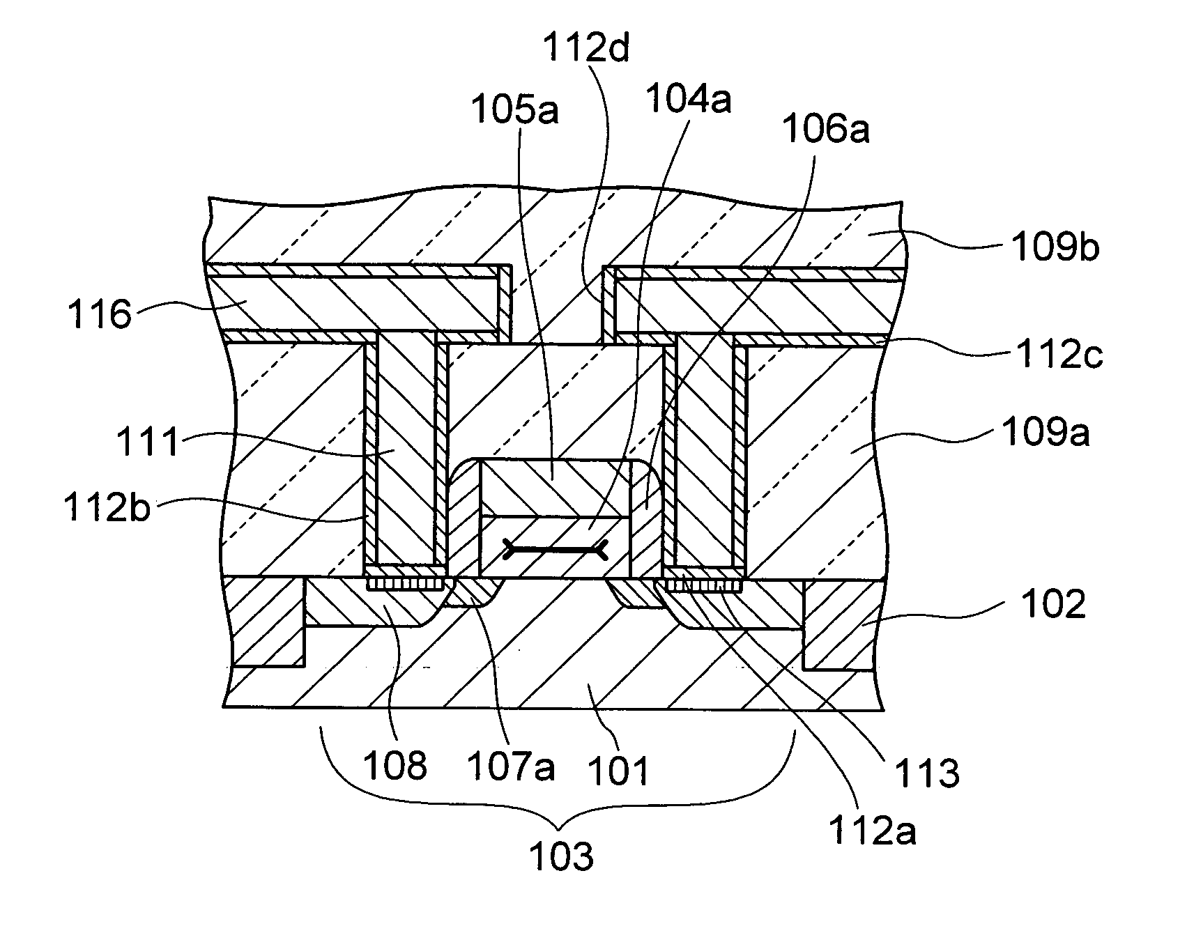
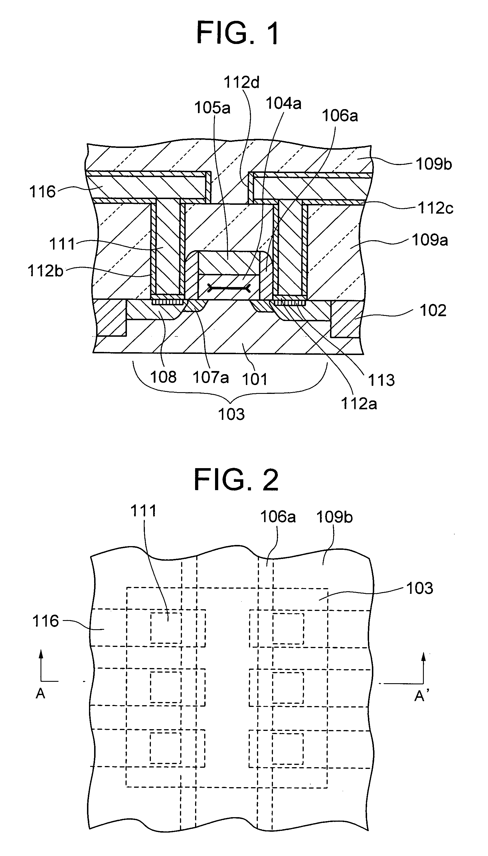
[0050] A sectional structure of a main portion of a semiconductor device according to a first embodiment of the present invention is shown in FIG. 1, which is a sectional view taken along A-A′ in an example of a layout in a plan view shown in FIG. 2. The semiconductor device of the embodiment includes, as shown in FIG. 1, a device separation layer 102 of silicon oxide layer formed in the surface of a P-type silicon substrate 101 and a device formation area 103. The embodiment shows the semiconductor device having an electric field effect type transistor by way of example. An N-channel MOS (NMOS) transistor is formed in the device formation area 103.

[0051] The MOS transistor includes a gate insulating layer 104a and a gate electrode 105a. A side wall 106a of silicon oxide, for example, is formed on the side of the gate electrode 105a. The gate insulating layer 104a is made of SiON. The gate electrode 105a is, for example, polycrystalline silicon layer, metal thin film layer, metal s...

embodiment 2

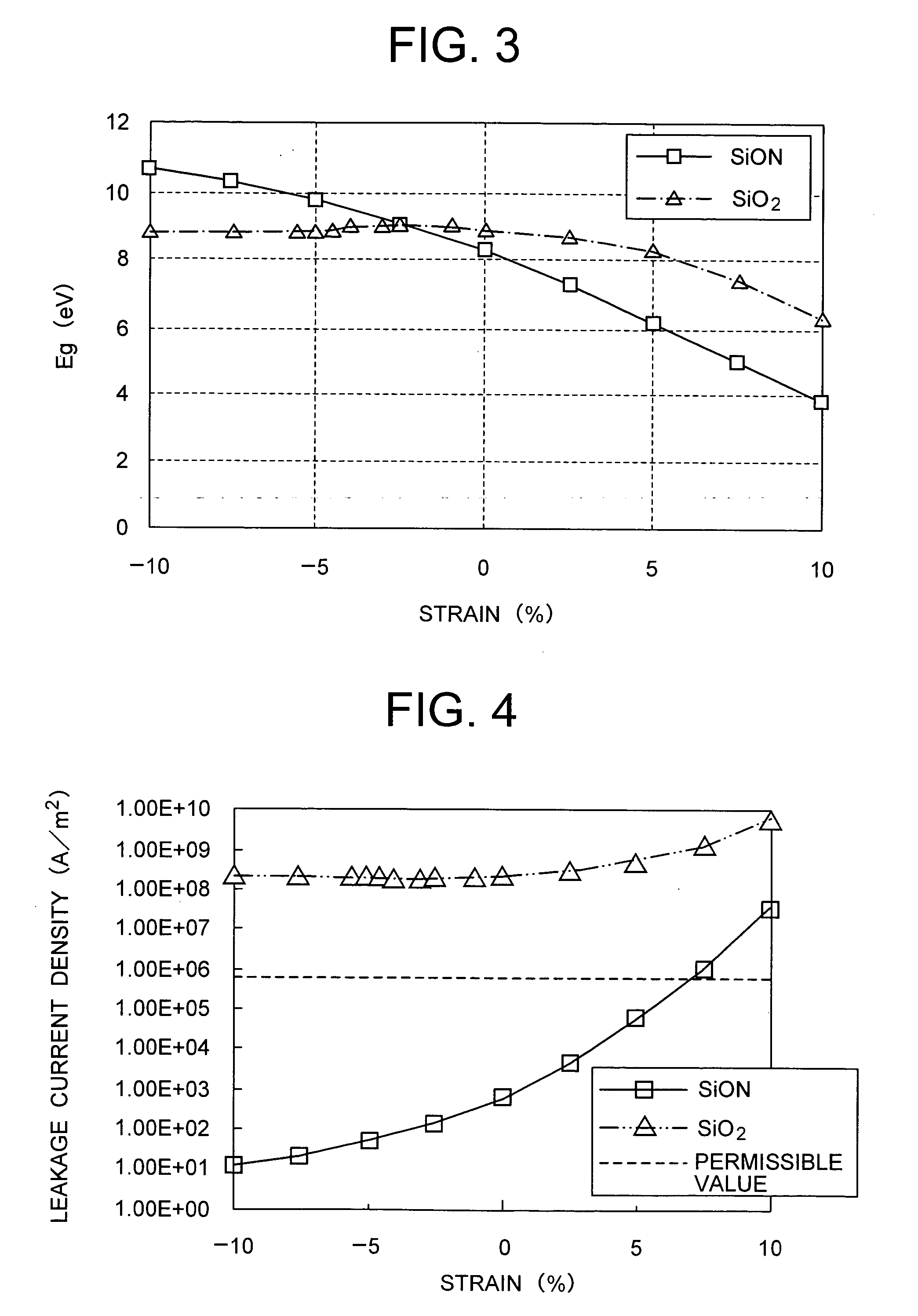
[0065] A second embodiment of the present invention is now described with reference to FIGS. 6A to 6D and FIGS. 7A to 7C. In order to make the gate insulating layer to the compressed strain state, the gate electrode is made to the tensile strain state, for example. The gate electrode is made to the tensile strain state, so that the gate insulating layer disposed under the gate electrode is formed to be made to the compressed strain state as a result of its reaction.

[0066]FIGS. 6A to 6D and FIGS. 7A to 7C illustrate the manufacturing method of the semiconductor device including the gate electrode in the tensile strain state and the SiON gate insulating layer in the compressed strain state.

[0067] First, groove having the depth of 200 to 300 nm are formed in the surface of a P-type silicon substrate 101 and silicon oxide layer is embedded therein to form device separation layer 102 of shallow groove type (FIG. 6A).

[0068] Next, the surface of the silicon substrate 101 is thermally ox...

embodiment 3

[0085] In the embodiment 3, after formation of the SiON layer by the thermal oxidization of the surface of the silicon substrate 101 in the embodiment 2, an amorphous silicon layer 115 containing impurity phosphorus (P) is formed by means of the CVD method or the like.

[0086] Thereafter, the temperature of the semiconductor substrate is raised to 600° C. or more so that the amorphous silicon layer 115 is crystallized to be the polycrystalline silicon layer 105. Since the crystallization of the amorphous silicon contracts its volume, the polycrystalline silicon layer 105 formed by the crystallization becomes the tensile strain state. As a result of the reaction of the tensile strain, the SiON gate insulating layer 104 under the polycrystalline silicon layer 105 becomes the compressed strain state (FIG. 6D). The crystallization of the amorphous silicon layer 115 can be made by controlling the temperature of the semiconductor substrate, although it may be made by irradiation of laser. ...


PUM


Abstract

A semiconductor device constitutes an electric field effect type transistor having a semiconductor substrate, a gate insulating layer formed on the substrate and a gate electrode formed on the gate insulating layer. The gate insulating layer is mainly formed of silicon oxynitride (SiON) and a strain state of the gate insulating layer is a compressed strain state.

Description

BACKGROUND OF THE INVENTION [0001] The present invention relates to a semiconductor device. [0002] Silicon dioxide (SiO2) has excellent insulation properties having a band gap as large as 8 to 9 eV and is often used as material for gate insulating layers, inter-layer insulating layers or the like in a semiconductor device. [0003] However, recently, gate insulating layers are required to be thinned due to miniaturization of semiconductor devices and oxide layers having the thickness of 3.0 nm or less are used. When the thickness of the oxide layers is thinned to 3.0 nm or less, there is a problem that a tunnel current is increased as it cannot be disregarded, so that a leakage current is increased to thereby increase the power consumption. [0004] It is known that the tunnel current is mainly divided into a Fowler-Nordheim tunnel current (FN current) and a direct tunnel current (DT current). The FN current is the current flowing by causing electrons to tunnel the triangle potential ge...

Claims


Application Information

Patent Timeline
IPC IPC(8): H01L21/283H01L21/28H01L21/314H01L21/3205H01L21/8234H01L21/8238H01L21/8247H01L23/52H01L27/04H01L27/088H01L27/115H01L29/417H01L29/51H01L29/76H01L29/78H01L29/788H01L29/792
CPCH01L21/28035H01L21/28202H01L21/823456H01L21/823462H01L21/82385H01L29/7881H01L27/115H01L27/11521H01L29/518H01L29/7842H01L29/7845H01L21/823857H10B69/00H10B41/30
Inventor KANEGAE, YOSHIHARUIWASAKI, TOMIOMORIYA, HIROSHI
Owner HITACHI LTD
Why Eureka
Try Eureka