Waveguide device having improved spatial filter configurations

a waveguide and spatial filter technology, applied in the field of electronic waveguide devices, can solve the problems of only two optical paths (i.e., primary and secondary paths) traveled by unguided light, affecting the desired optical signal, and limiting the number of obstructed light paths

Active Publication Date: 2007-08-30
HONEYWELL INT INC
View PDF2 Cites 7 Cited by
  • Summary
  • Abstract
  • Description
  • Claims
  • Application Information

AI Technical Summary

Problems solved by technology

In one known waveguide device, specifically a proton exchange polarizer, the PER is increased employing a spatial filter to block two optical paths (i.e., the primary and secondary optical paths) that the unguided transverse magnetic (TM) mode light may travel and be received at the output fiber, thus interfering with the desired optical signal.
Unfortunately, spatial filter arrangements of the type described above typically block only two optical path

Method used


Image

  • Waveguide device having improved spatial filter configurations
  • Waveguide device having improved spatial filter configurations
  • Waveguide device having improved spatial filter configurations

Examples


first embodiment

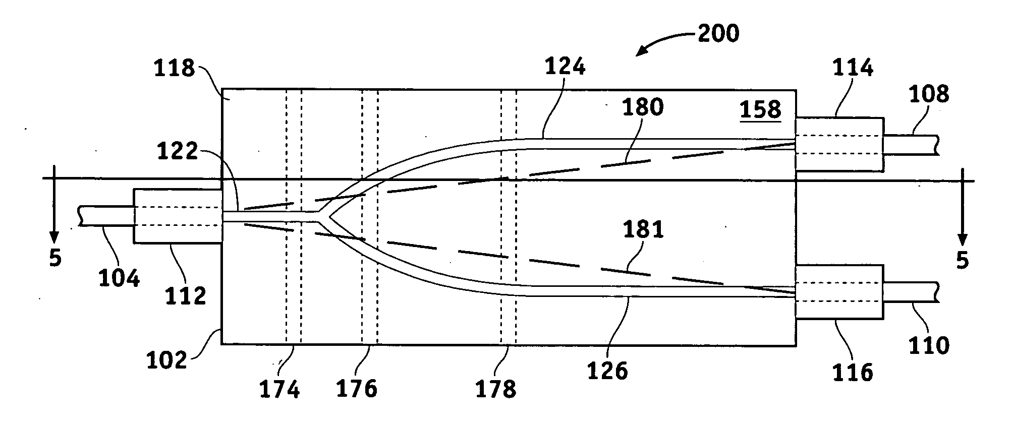
[0026]FIGS. 4-6 illustrate the present invention; i.e., an optical modulator 200 wherein three baffles 174, 176, and 178 having substantially rectangular cross-sections are provided within substrate 118 at different locations along bottom surface 148. In particular, FIGS. 4, 5, and 6 are a top view, a side cross-sectional view taken along line 5-5 of FIG. 4, and a bottom view of modulator 200, respectively. Referring FIGS. 4-6, assuming substrate 118 has a length of X, baffles 174, 176, and 178 may be disposed approximately distances (⅛)X, (¼)X, and (½)X, respectively, from first end 102 of substrate 118. Described another way, baffles 174, 176, and 178 are positioned proximate respective transverse reflection points 162, 152, and 146 discussed above in conjunction with FIG. 3. As FIG. 5 illustrates, by positioning baffles 174, 176, and 178 in this manner, this embodiment of modulator 200 substantially blocks the primary, secondary, and tertiary reflection optical paths 174, 176, an...

second embodiment

[0027]FIGS. 7-9 are a top, side cross-sectional (taken along line 8-8 of FIG. 7), and bottom views, respectively, of the present invention. In optical modulator 210, two baffles 212 and 214 having a substantially rectangular cross-section are provided within substrate 118 along bottom surface 148. In addition, two narrow baffles 216 and 218 having saw-tooth cross-sections are provided within substrate 118 along upper surface 158. As may be appreciated by comparing FIGS. 7-9 to FIGS. 4-6, baffles 212 and 214 are disposed within optical modulator 200 in substantially the same position as are baffles 176 and 178 within optical modulator 210 and thus substantially block optical paths 150 and 144, respectively, as described above. In contrast to modulator 200, however, optical path 160 is substantially blocked by narrow baffles 216 and 218 (FIG. 8). In addition, narrow baffles 216 and 218 substantially block direct optical paths 180 and 181 (FIGS. 7 and 8). If substrate 118 has a length ...

third embodiment

[0028]FIGS. 10-12 are top, side cross-sectional (taken along line 11-11 of FIG. 10), and bottom views, respectively, of the present invention. In optical modulator 220, a first baffle 222 having a substantially rectangular cross-section is provided within substrate 118 proximate bottom surface 148, and a second baffle 224 is provided within substrate 118 proximate upper surface 158. Longitudinally, baffles 222 and 224 are each positioned at approximately the middle region of substrate 118. Baffle 224 is disposed so as to block the optical paths traveling directly from inlet fiber 104 to outlet fibers 108 and 110 (i.e., optical paths 180 and 181) in addition to optical reflection paths 150 and 160. Baffle 222 is disposed so as to block optical path 144 in the manner described above. It should thus be appreciated that the embodiment shown in FIGS. 10-12 is configured to impede or block substantially all of the major optical paths along which unguided light may travel (i.e., the primar...


PUM


Abstract

An optical waveguide device is provided for receiving light that has a guided mode and an unguided mode. The device comprises an optically transmissive substrate having first and second substantially opposite surfaces, an input end, and an output end. An optical waveguide region is disposed within the substrate and extends from the input to the output. A plurality of electrodes is disposed on the first surface at predetermined locations with respect to the waveguide region. The device includes a plurality of optical barriers each disposed proximate one of the first and second surfaces and positioned to block a different optical path of the unguided mode.

Description

STATEMENT REGARDING FEDERALLY SPONSORED RESEARCH OR DEVELOPMENT [0001] This invention was made with Government support under contract no. N00030-05-C-0007 awarded by the Department of the Navy. The Government has certain rights in this invention.FIELD OF THE INVENTION [0002] The present invention generally relates to electro-optic waveguide devices and, more particularly, to a waveguide device having an improved spatial filter for blocking reflected light. BACKGROUND OF THE INVENTION [0003] Optical communications systems (e.g., integrated optic or multi-functional chips) now routinely employ electro-optic devices that utilize electrodes to modulate optical signals propagating through a waveguide formed in an optically transmissive substrate and optically coupled between an input optical fiber and one or more output optical fibers. The substrate typically comprises an electro-optic crystal, such as lithium niobate (LiNbO3), that transmits substantially polarized light and undergoes a...

Claims


Application Information

Patent Timeline
IPC IPC(8): G02B6/26
CPCG02B6/125G02F1/3137G02F1/035G02B6/126
Inventor LANGE, CHARLES H.
Owner HONEYWELL INT INC
Why Eureka
Try Eureka