Liquid crystal display device

Active Publication Date: 2007-10-18
PANASONIC LIQUID CRYSTAL DISPLAY CO LTD +1
View PDF11 Cites 11 Cited by
  • Summary
  • Abstract
  • Description
  • Claims
  • Application Information

AI Technical Summary

Benefits of technology

[0031]An advantageous effect obtained by the typical aspects of the invention disclosed in this application is briefly des

Problems solved by technology

However, as also described in Japanese Patent Application Laid-Open Publication No. 2003-344837, when a semi-transmissive liquid crystal display device is constructed using an IPS liquid crystal display device, for example, ther

Method used


Image

  • Liquid crystal display device
  • Liquid crystal display device
  • Liquid crystal display device

Examples


first embodiment

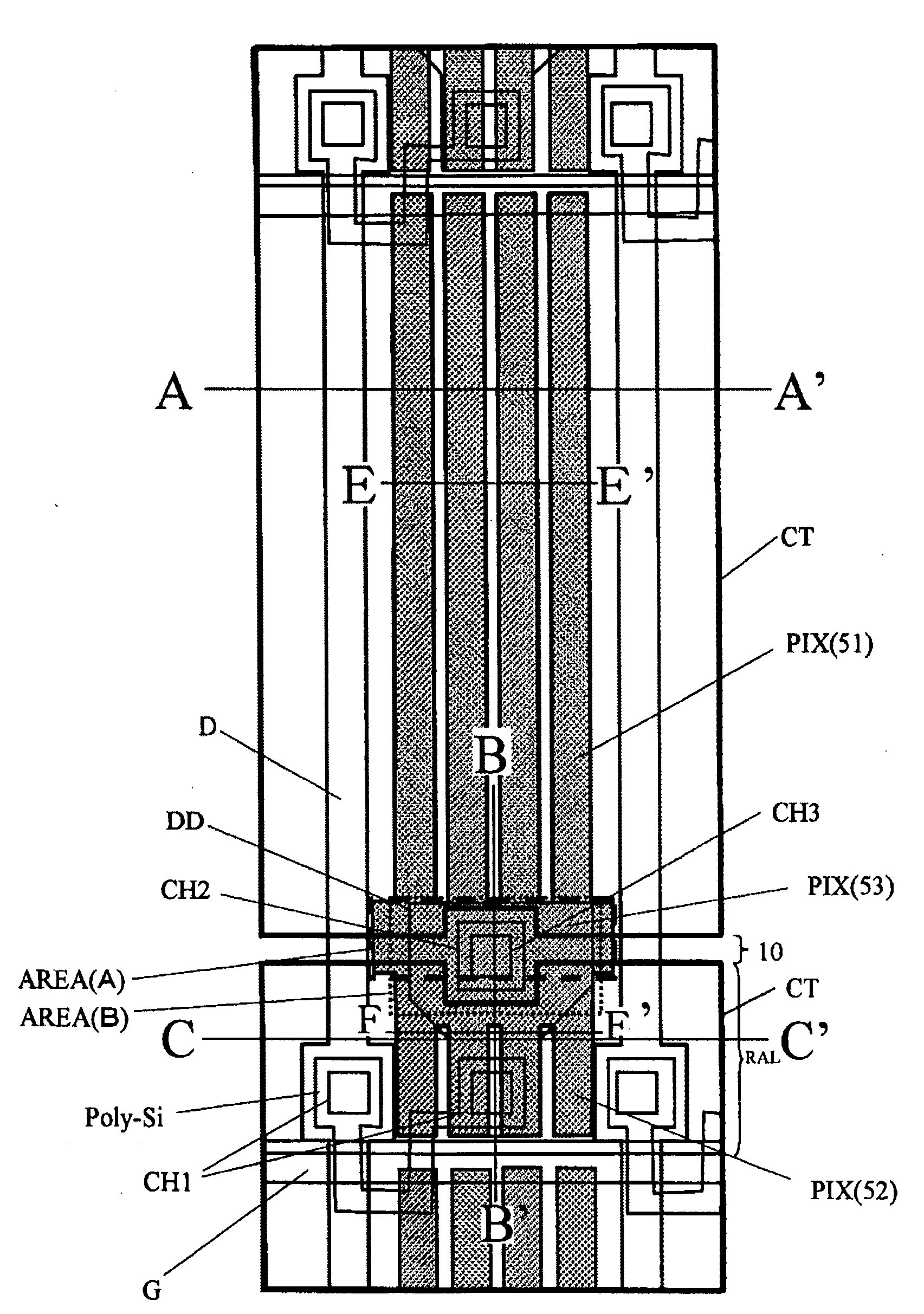
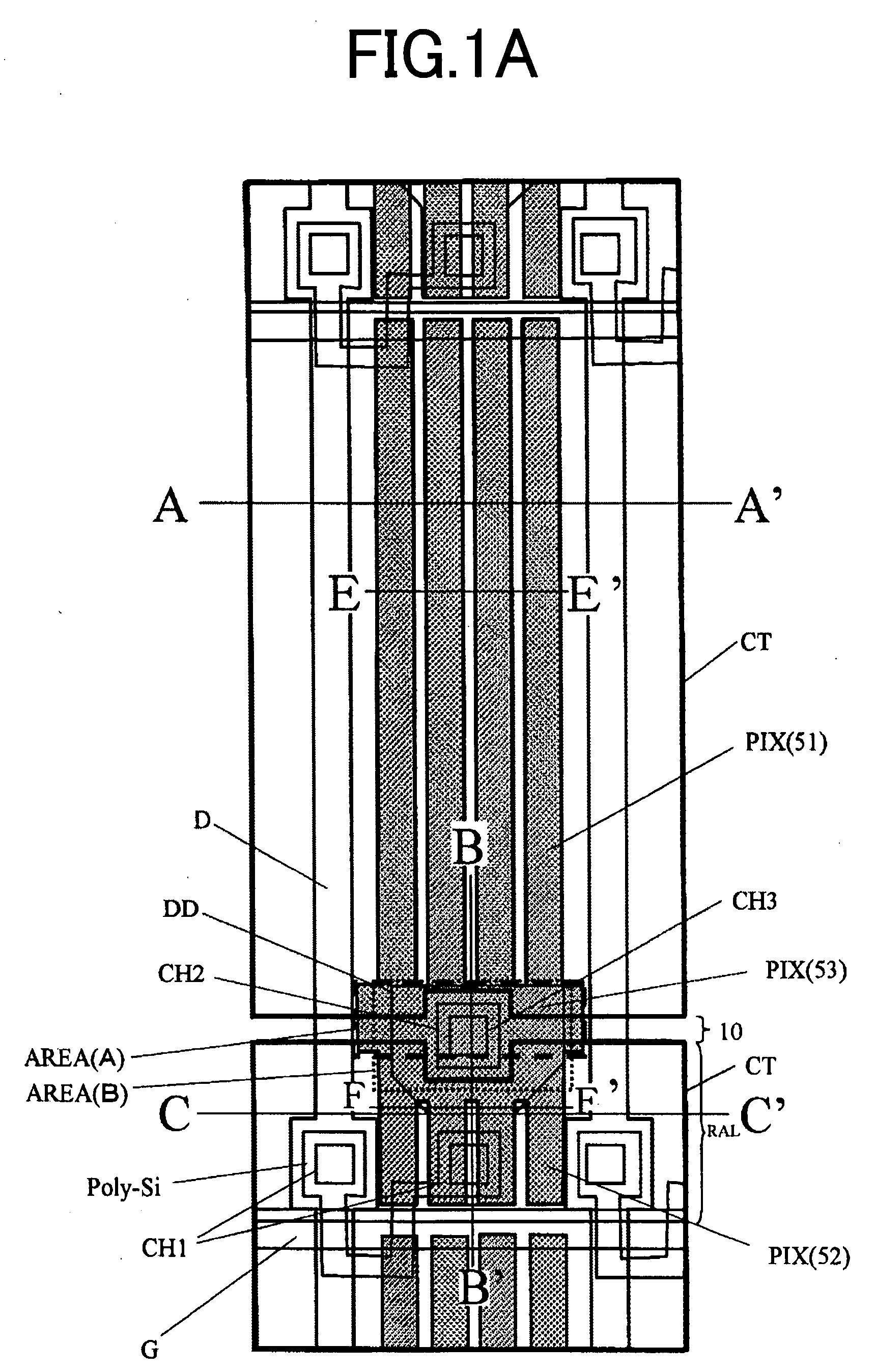
[0061]FIG. 1A is a plan view showing the electrode structure of a subpixel of a semi-transmissive liquid crystal display device according to a first embodiment of the present invention.

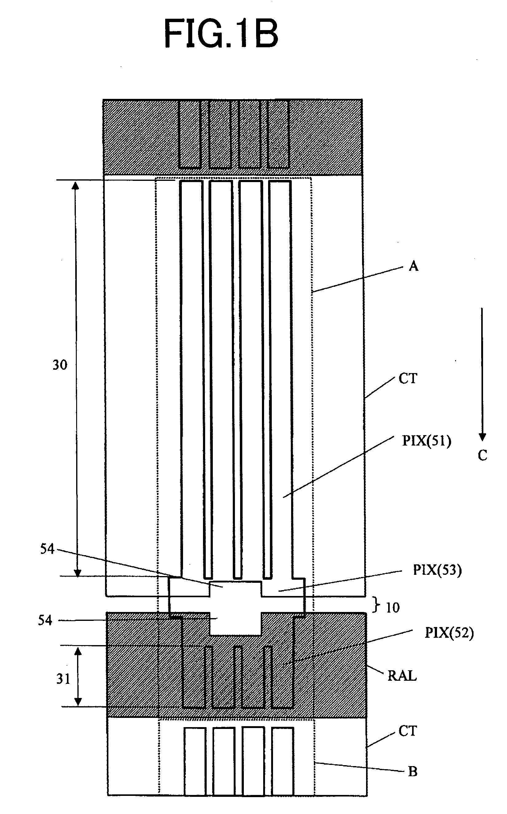
[0062]FIG. 1B is a drawing showing only a pixel electrode, a counter electrode, and a reflection electrode among elements shown in FIG. 1A. In FIG. 1B, parts shown by dotted frames A and B each represent one subpixel.

[0063]Also in one subpixel of the semi-transmissive liquid crystal display device according to this embodiment, as shown in FIG. 1B, the transmission section 30 and reflection section 31 share one pixel electrode PIX and each have an independent counter electrode CT. In other words, a counter electrode CT is divided into two counter electrodes: one for the transmission section and another for the reflection section. A reflection electrode RAL is formed on the counter electrode CT for the reflection section 31.

[0064]In FIG. 1B, one electrode is shared by the counter electrode CT for the re...

second embodiment

[0116]FIG. 8 is a plan view showing the electrode structure of a subpixel of a semi-transmissive liquid crystal display device according to a second embodiment of the present invention.

[0117]As shown by DW in FIG. 8, the semi-transmissive liquid crystal display device according to this embodiment is different from that according to the first embodiment shown in FIG. 1A in that the video line D is partially thickened below the clearance 10 and the connection 53 of the pixel electrode PIX.

[0118]The semi-transmissive liquid crystal display device according to this embodiment will now be described below focusing on the differences from that according to the first embodiment.

[0119]If the clearance 10 between the opposed counter electrodes CT is covered by the pixel electrode PIX as in the first embodiment, the pixel electrode PIX comes close to a connection 53 of an adjacent subpixel because the connection 53 of the pixel electrode PIX extends in the transverse direction (direction of ex...


PUM


Abstract

A liquid crystal display device having a liquid crystal display panel includes a first substrate, a second substrate, and liquid crystal interposed between the first and second substrates. The first substrate includes an active element, a first insulating film formed on the active element, a plurality of first electrodes disposed on the first insulating film, a second insulating film disposed on the first electrodes, and a pixel electrode disposed on the second insulating film. The pixel electrode is electrically coupled to the active element via a portion defining a contact hole formed in a portion defining a clearance between the plurality of first electrodes.

Description

CLAIM OF PRIORITY[0001]The present application claims priority from Japanese Application JP 2006-109659 filed on Apr. 12, 2006, the content of which is hereby incorporated by reference into this application.BACKGROUND OF THE INVENTION[0002](1) Field of the Invention[0003]The present invention relates to a liquid crystal display device, particularly to an in-plane switching (hereinafter referred to as “IPS”), semi-transmissive liquid crystal display device.[0004](2) Description of the Related Art[0005]Semi-transmissive liquid crystal display devices that have a transmission section and a reflection section in a subpixel have been used as displays for portable devices.[0006]These semi-transmissive liquid crystal display devices employ the vertical electric field method in which liquid crystal interposed between a pair of substrates is driven by applying an electric field in a direction perpendicular to the planes of the pair of substrates. Those display devices have a step between the...

Claims


Application Information

Patent Timeline
IPC IPC(8): H01L29/04
CPCG02F1/133555G02F1/134363H01L27/12G02F1/136286G02F2201/40G02F1/136227
Inventor OCHIAI, TAKAHIRONAKAO, TAKAYUKIMIYAZAWA, TOSHIOMAKI, MASAHIROSASAKI, TOHRU
Owner PANASONIC LIQUID CRYSTAL DISPLAY CO LTD
Why Eureka
Try Eureka