Semiconductor component having a curved mirror and method for producing a semiconductor component having a curved semiconductor body

Inactive Publication Date: 2007-10-25
OSRAM OPTO SEMICON GMBH & CO OHG
View PDF11 Cites 2 Cited by
  • Summary
  • Abstract
  • Description
  • Claims
  • Application Information

AI Technical Summary

Benefits of technology

[0004] It is an object of the invention to provide a semiconductor component havin

Problems solved by technology

The alignment of the curved mirror in three-dimensional space is often complicated, however, for an efficient laser activity, in particular in the fundamental mode, of the

Method used


Image

  • Semiconductor component having a curved mirror and method for producing a semiconductor component having a curved semiconductor body
  • Semiconductor component having a curved mirror and method for producing a semiconductor component having a curved semiconductor body
  • Semiconductor component having a curved mirror and method for producing a semiconductor component having a curved semiconductor body

Examples


Example

DETAILED DESCRIPTION OF THE DRAWINGS

[0060] Elements that are identical, of identical type or act identically are provided with the same reference symbols in the figures.

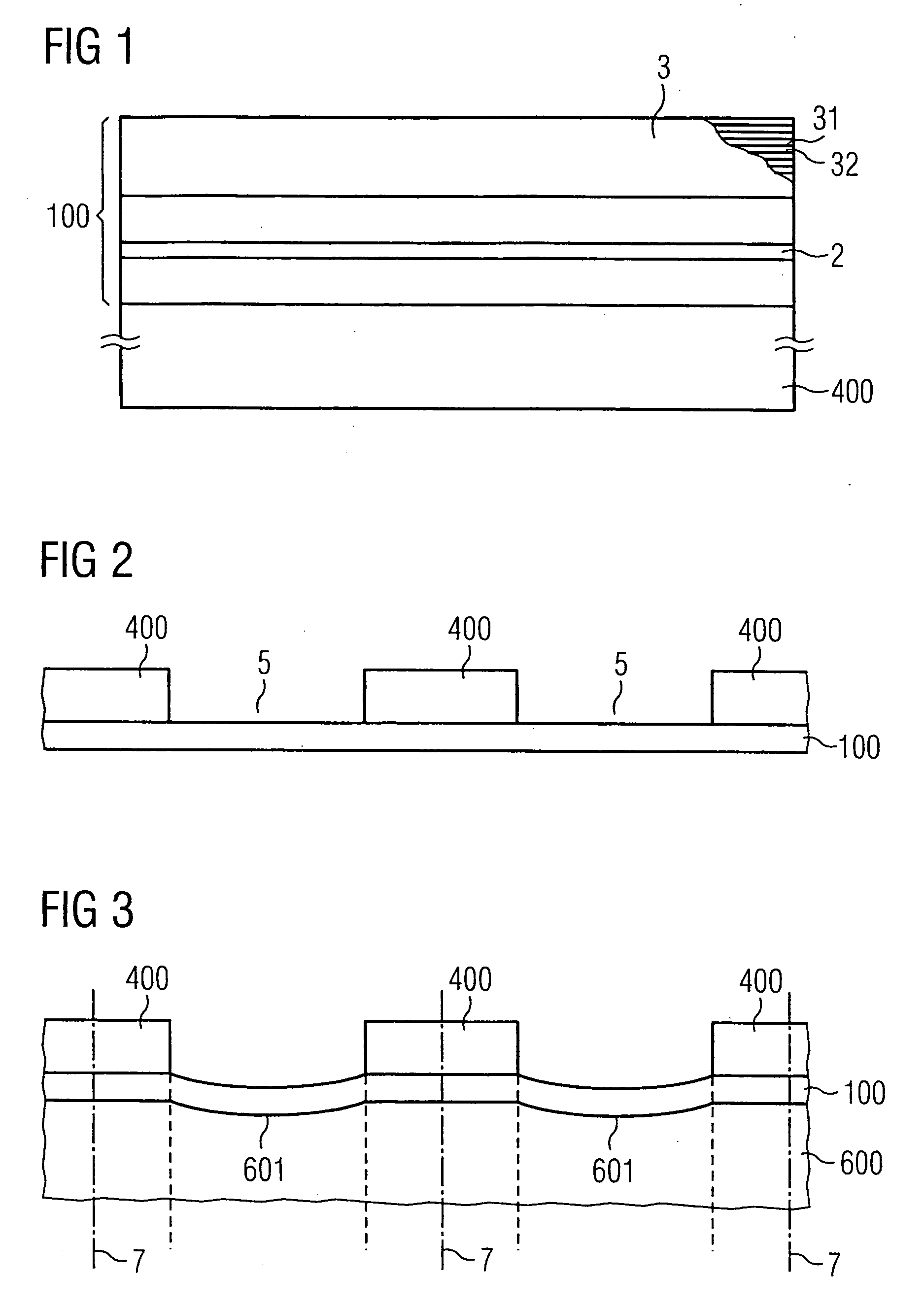
[0061] FIGS. 1 to 3 schematically illustrate a first exemplary embodiment of a method according to the invention on the basis of intermediate steps shown in the figures.

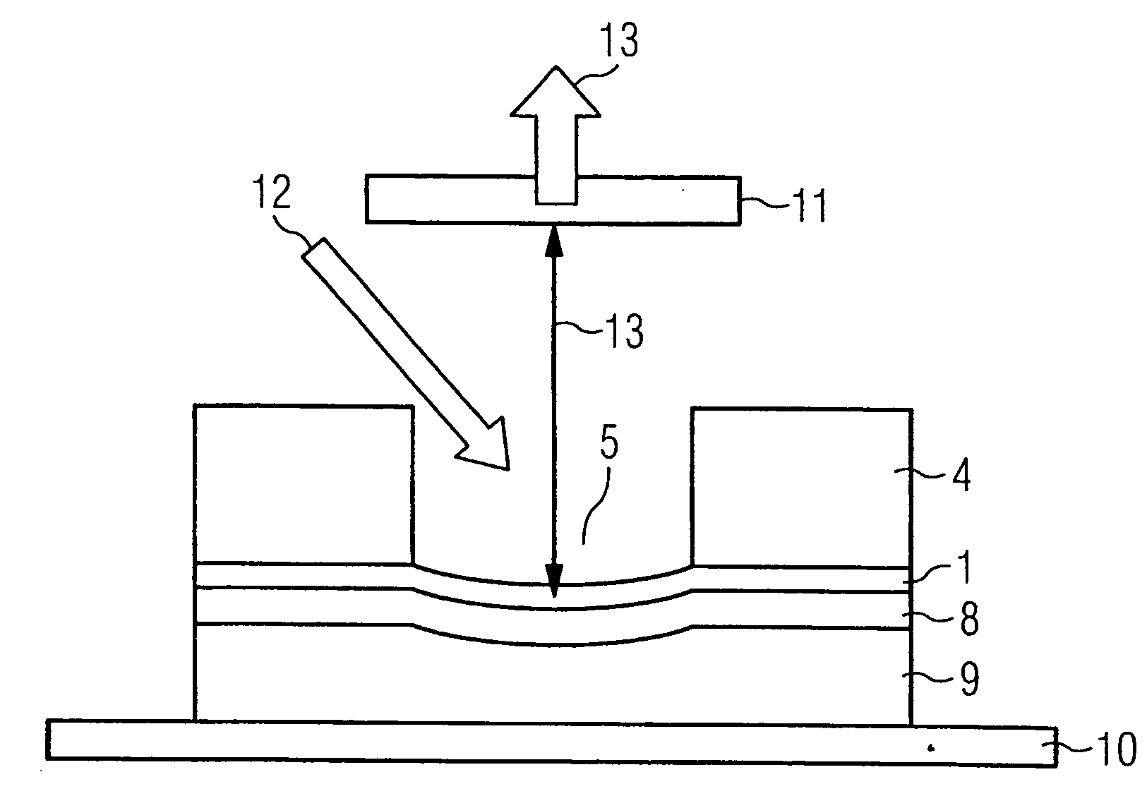
[0062] Firstly, as shown in FIG. 1, provision is made of a semiconductor layer sequence 100 arranged on a carrier layer 400, said semiconductor layer sequence comprising an active zone 2 provided for the generation of radiation and a mirror structure 3. The mirror structure 3 is integrated with the active zone 2, in particular monolithically in the semiconductor layer sequence.

[0063] The carrier layer 400 is provided for example by the growth substrate on which the semiconductor layer sequence was grown epitaxially, or may comprise the growth substrate. If appropriate, however, the carrier substrate may also differ from the growth substrate. The s...


PUM


Abstract

A semiconductor component having a semiconductor body, the semiconductor body comprising a curved mirror (3), which is monolithically integrated in the semiconductor body. A method for curving a semiconductor body is also disclosed.

Description

RELATED APPLICATIONS [0001] This patent application claims the priority of German patent application nos. 10 2004 040 762.2 and 10 2004 052 686.9 filed Aug. 23, 2004 and Oct. 29, 2004, respectively, the disclosure content of which is hereby incorporated by reference. FIELD OF THE INVENTION [0002] The invention relates to a semiconductor component having a curved mirror and to a method for producing a semiconductor component having a curved semiconductor body. BACKGROUND OF THE INVENTION [0003] In the case of surface emitting semiconductor lasers with an external resonator and a vertical emission direction with respect to the surface of a semiconductor body of the laser, for example a VECSEL (Vertical External Cavity Surface Emitting Laser) or semiconductor disk laser, the external resonator is often formed by a planar Bragg mirror integrated in the semiconductor body of the semiconductor laser and a curved external dielectric mirror. Fundamental mode operation of the laser can be ob...

Claims


Application Information

Patent Timeline
IPC IPC(8): H01L29/06H01L33/00H01L31/00H01L31/12H01L29/22H01L27/15
CPCH01S3/109H01S5/0224H01S5/041H01S5/4056H01S5/18383H01S5/18388H01S5/141H01S5/0234
Inventor REILL, WOLFGANGSTEEGMULLER, ULRICHALBRECHT, TONYSCHMID, WOLFGANG
Owner OSRAM OPTO SEMICON GMBH & CO OHG
Why Eureka
Try Eureka