Stencil assembly structure

a technology of assembly structure and stencil, which is applied in the direction of coating, printing, circuit masks, etc., can solve the problems of deteriorating printing quality, unsatisfactory printing quality, and use of assembled solder paste printing structure, so as to reduce the possibility of detaching solder paste and improve printing quality. , the effect of simple and cost-effectiv

Active Publication Date: 2015-08-27
DELTA ELECTRONICS (THAILAND) PUBLIC CO LTD
View PDF11 Cites 2 Cited by
  • Summary
  • Abstract
  • Description
  • Claims
  • Application Information

AI Technical Summary

Benefits of technology

[0008]The present invention provides a stencil assembly structure for printing solder paste on a printed circuit board. The stencil assembly structure can be fabricated in a simplified and cost-effective manner. Moreover, the tension of the stencil can be uniformly adjusted to be maintained at a sufficient level and uniform distribution. Under this circumstance, the possibility of detaching the solder paste is minimized, and the printing quality is enhanced.

Problems solved by technology

That is, if the tension is insufficient, the printing quality is deteriorated.
However, the use of the conventional assembled solder paste printing structure still has some drawbacks.
For example, since the tension is not uniformly and properly distributed on the rectangular steel plate, the printing quality is usually unsatisfied.
Moreover, after the conventional assembled solder paste printing structure has been used for a certain time period, the tension of the rectangular steel plate is possibly destroyed and impaired.
Moreover, since the conventional assembled solder paste printing structure cannot be disassembled, the conventional assembled solder paste printing structure fails to match various printed circuit boards.
Under this circumstance, the assembling process is complicated, and the assembling cost is increased.

Method used


Image

  • Stencil assembly structure
  • Stencil assembly structure
  • Stencil assembly structure

Examples


Embodiment Construction

[0035]The present invention will now be described more specifically with reference to the following embodiments. It is to be noted that the following descriptions of preferred embodiments of this invention are presented herein for purpose of illustration and description only. It is not intended to be exhaustive or to be limited to the precise form disclosed.

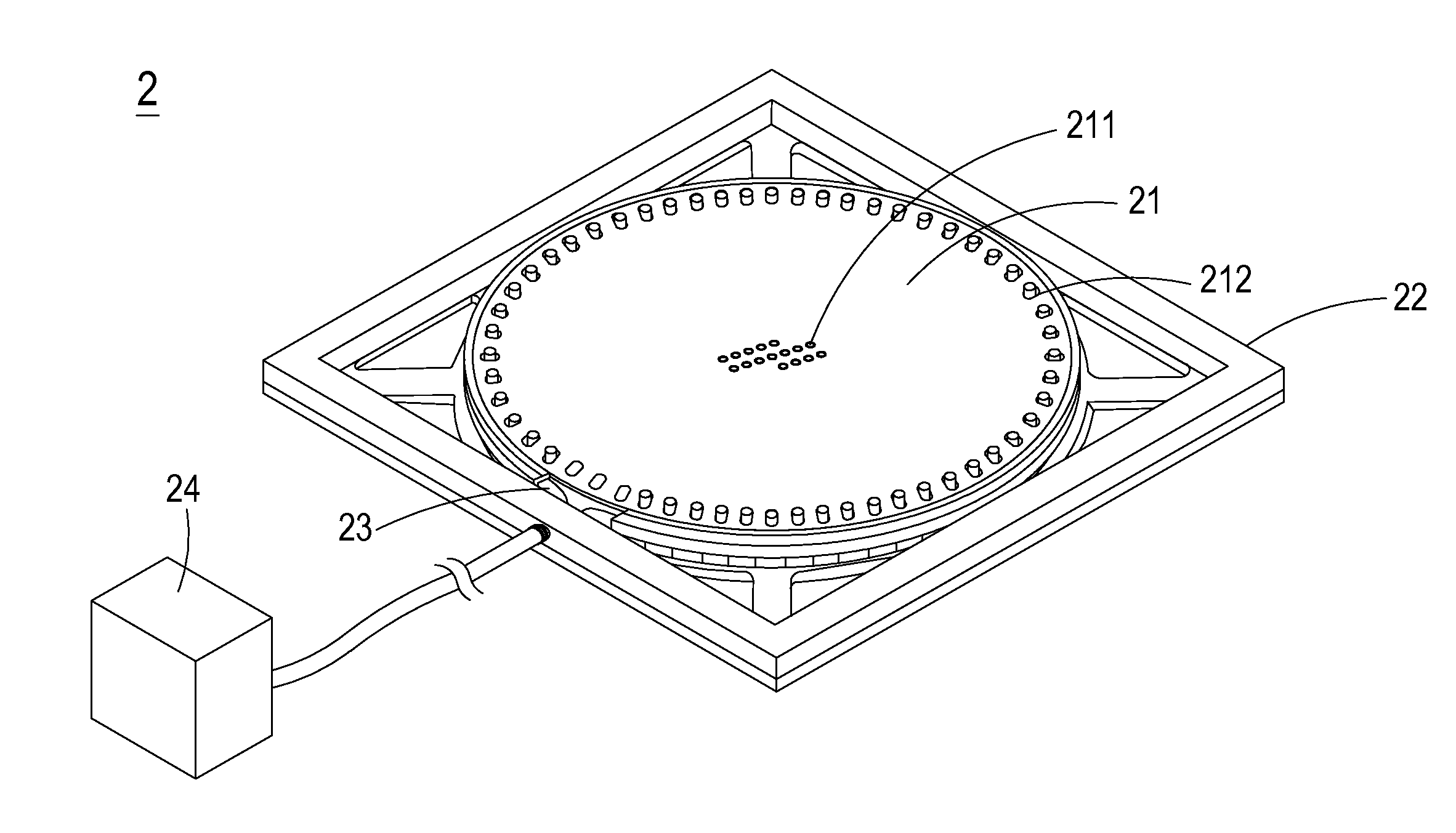
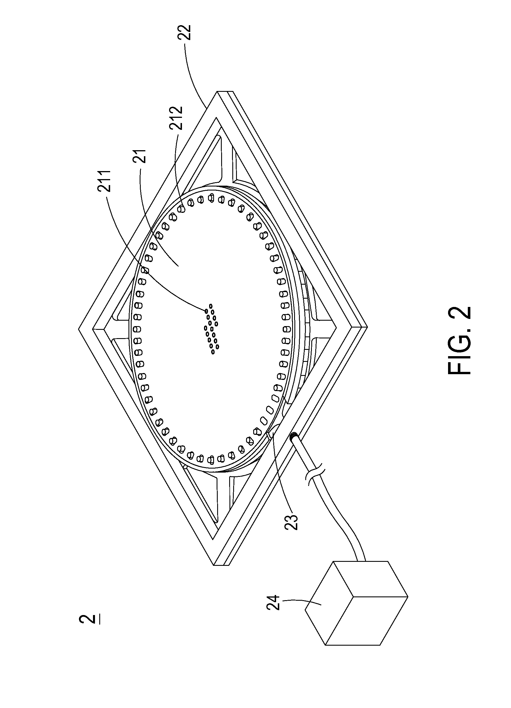
[0036]FIG. 2 is a schematic view illustrating a stencil assembly structure according to an embodiment of the present invention and FIG. 3 is a schematic exploded view illustrating the stencil assembly structure according to the embodiment of the present invention. As shown in FIG. 2 and FIG. 3, the stencil assembly structure 2 comprises a stencil 21, a fixing frame 22, a deformable tube 23 and a gas supplying device 24. The stencil 21 comprises plural first apertures 211 and plural second apertures 212. The plural first apertures 211 are formed by a laser cutting process, and collaboratively defined as a solder paste printing pat...


PUM


Abstract

A stencil assembly structure used for printing solder paste on a printed circuit board includes a stencil, a fixing frame, a deformable tube and a gas supplying device. The stencil includes plural first apertures and plural second apertures. The plural first apertures are collaboratively defined as a solder paste printing region. The fixing frame includes a frame body and plural fixing seats, and each fixing seat has a guide pin. After the plural guide pins are penetrated through the corresponding second apertures of the stencil, the stencil is fixed on the fixing seats. The deformable tube is disposed at bottoms of the fixing seats. The gas supplying device is connected with the deformable tube to adjust gas amount in the deformable tube. Due to deformation of the deformable tube resulted from gas pressure in the deformable tube, the guide pins are moved and a tension of the stencil is adjusted.

Description

CROSS-REFERENCE TO RELATED APPLICATIONS[0001]The present application is a continuation-in-part of U.S. patent application Ser. No. 14 / 156,074 entitled “STENCIL ASSEMBLY STRUCTURE” filed on Jan. 15, 2014, the entirety of which is hereby incorporated by reference.FIELD OF THE INVENTION[0002]The present invention relates to a stencil assembly structure, and more particularly to a stencil assembly structure for printing solder paste on a printed circuit board.BACKGROUND OF THE INVENTION[0003]A surface mount technology (SMT) is a method for mounting electronic components on the surface of a printed circuit board. The surface mount technology is capable of automatically fabricating small-sized, reliable, high-density and cost-effective electronic products. Generally, the solder paste printing pattern for the surface mount technology is defined by the apertures of a stencil. In addition, solder paste may pass through the apertures of the stencil to corresponding bonding pads of the printed...

Claims


Application Information

Patent Timeline
Patent Type & Authority Applications(United States)
IPC IPC(8): H05K3/00B05C21/00
CPCB05C21/005H05K3/0079B41F15/34B41F15/36B41L13/02B41F15/38
Inventor SURASIGCHA, RUAYSUKKHEE, PORNTHEP
Owner DELTA ELECTRONICS (THAILAND) PUBLIC CO LTD
Why Eureka
Try Eureka