Thermally enhanced BGA package with ground ring

a technology of ground ring and bga, which is applied in the direction of semiconductor devices, semiconductor/solid-state device details, electrical apparatus, etc., can solve the problems of thermal expansion and contraction of the package as a whole, and the concentration of excess heat generated during circuit operation, so as to improve the thermal path

Active Publication Date: 2007-10-25
TEXAS INSTR INC
View PDF5 Cites 15 Cited by
  • Summary
  • Abstract
  • Description
  • Claims
  • Application Information

AI Technical Summary

Benefits of technology

[0012] The invention has advantages including but not limited to providing an improved thermal path for the egress of heat from a packaged semiconductor device. This and other features, advantages, and benefits of the present invention can be understood by one of ordinary skill in the arts upon careful consideration of the detailed description of representative embodiments of the invention in connection with the accompanying drawings.

Problems solved by technology

All packages have drawbacks, however.
The high density of the flip-chip BGA which makes it desirable for many applications can lead to a concentration of excess heat generated during operation of the circuitry.
Due to the changes in temperature, the package as a whole tends to thermally expand and contract.
However, since in many cases the thermal expansion behavior of the packaged device, its internal components, and PCB differ, stresses can occur at the connecting solder balls, within the PCB or chip, or at the junctions of the package components.
A fairly direct thermal path exists from the front surface of the chip though the underlying substrate, however heat transmission is impaired by the generally poor thermal properties of the substrate itself.
This thermal path is sometimes improved by the addition of thermal vias or thermal BGA balls designed to increase heat conduction away from the chip and substrate respectively, but problems remain, particularly in the case of silicon on insulator (SOI) devices.
Although SOI devices typically generate less heat than other types of devices, ridding the SOI devices of excess heat is still a consideration, and the insulating layer is generally unhelpful in this regard.
The differences between the coefficients of thermal expansion of the silicon and oxide, glass, or other insulating layer(s) can result in stresses within the silicon layer(s), which tend to diminish electrical performance.
Additionally, stresses among and between the layers can cause mechanical separation leading to device failure.
This can be a fairly good thermal path, particularly in packages with thick substrates, but is generally longer and in some instances may be insufficient to adequately dissipate heat generated by the IC.
Current thermally enhanced flip-chip BGAs do not allow for electrical contact to the backside of the die.
Improvements to heat dissipation in BGA packages are necessarily limited by the geometry of the BGA and are not sufficient in all cases, leaving a need for further improvements in thermally enhanced BGA packages.

Method used


Image

  • Thermally enhanced BGA package with ground ring
  • Thermally enhanced BGA package with ground ring
  • Thermally enhanced BGA package with ground ring

Examples


Embodiment Construction

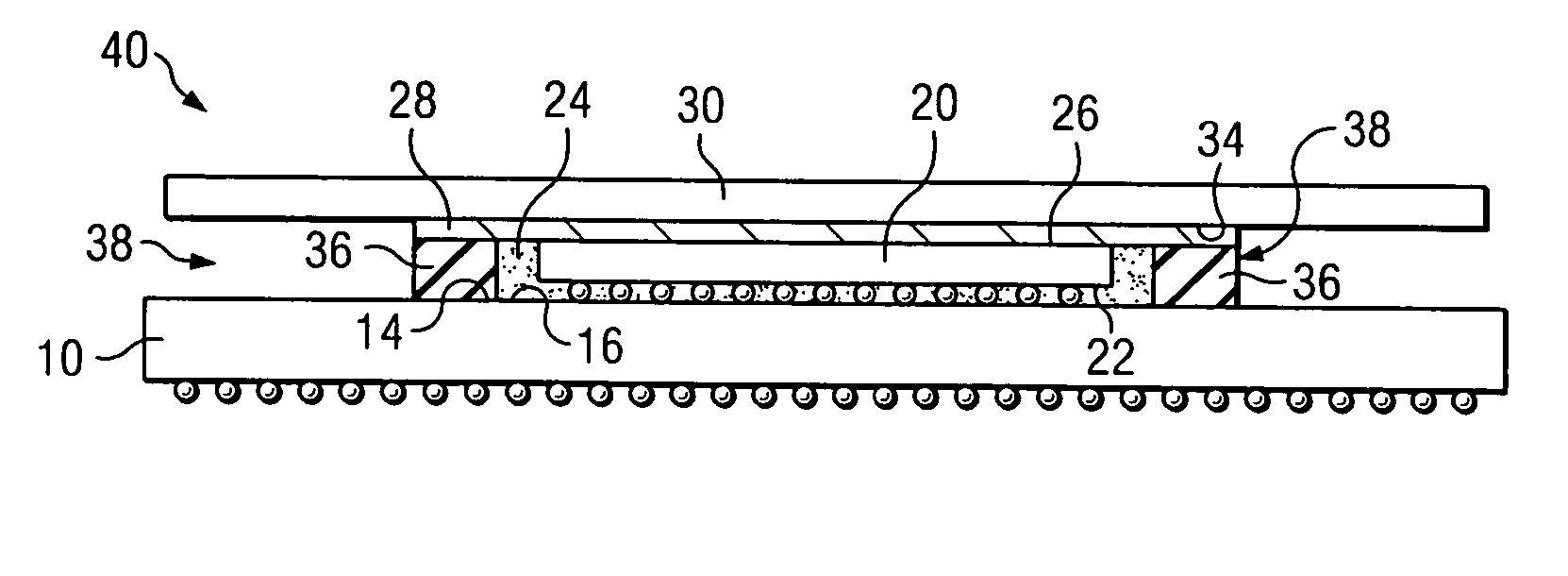
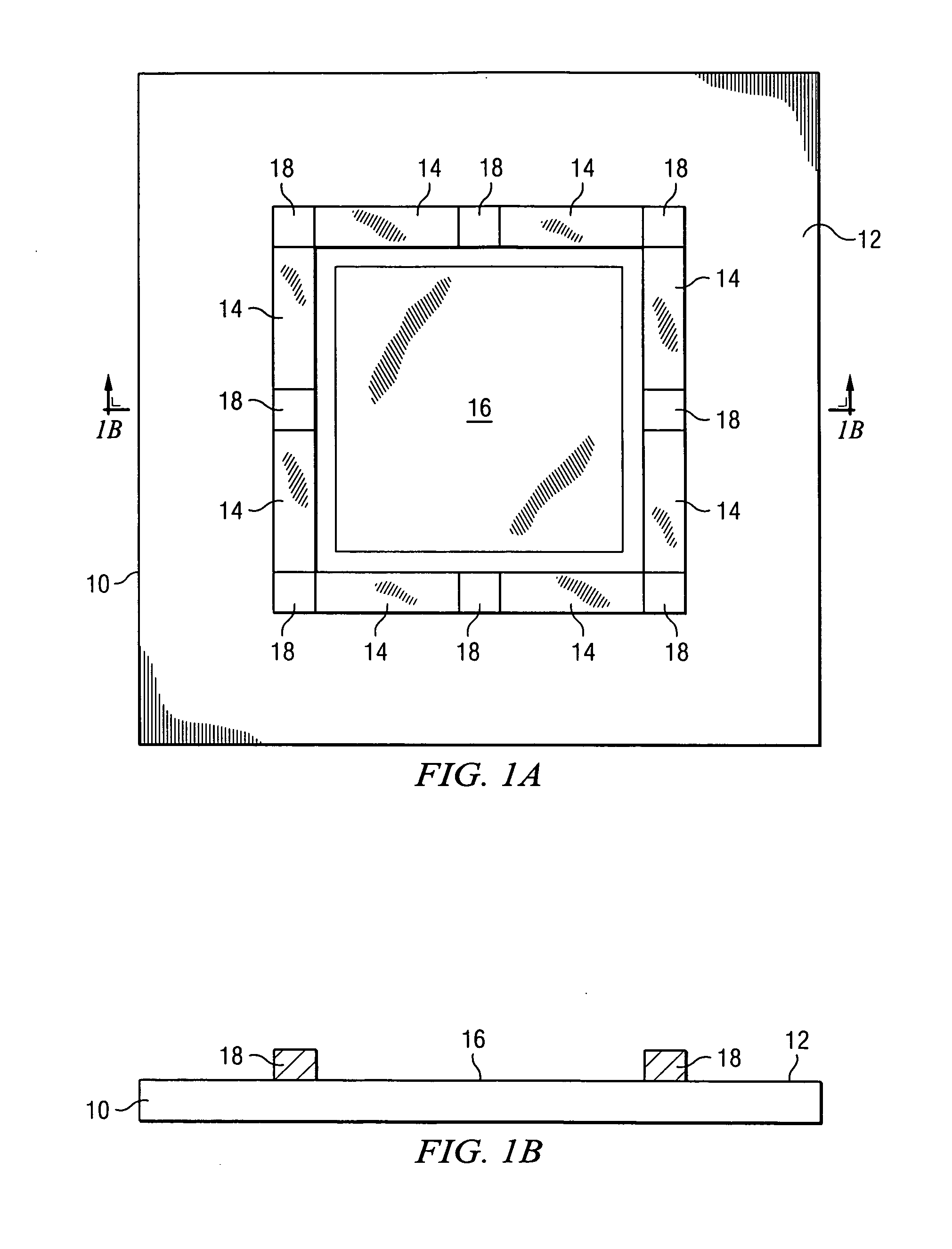
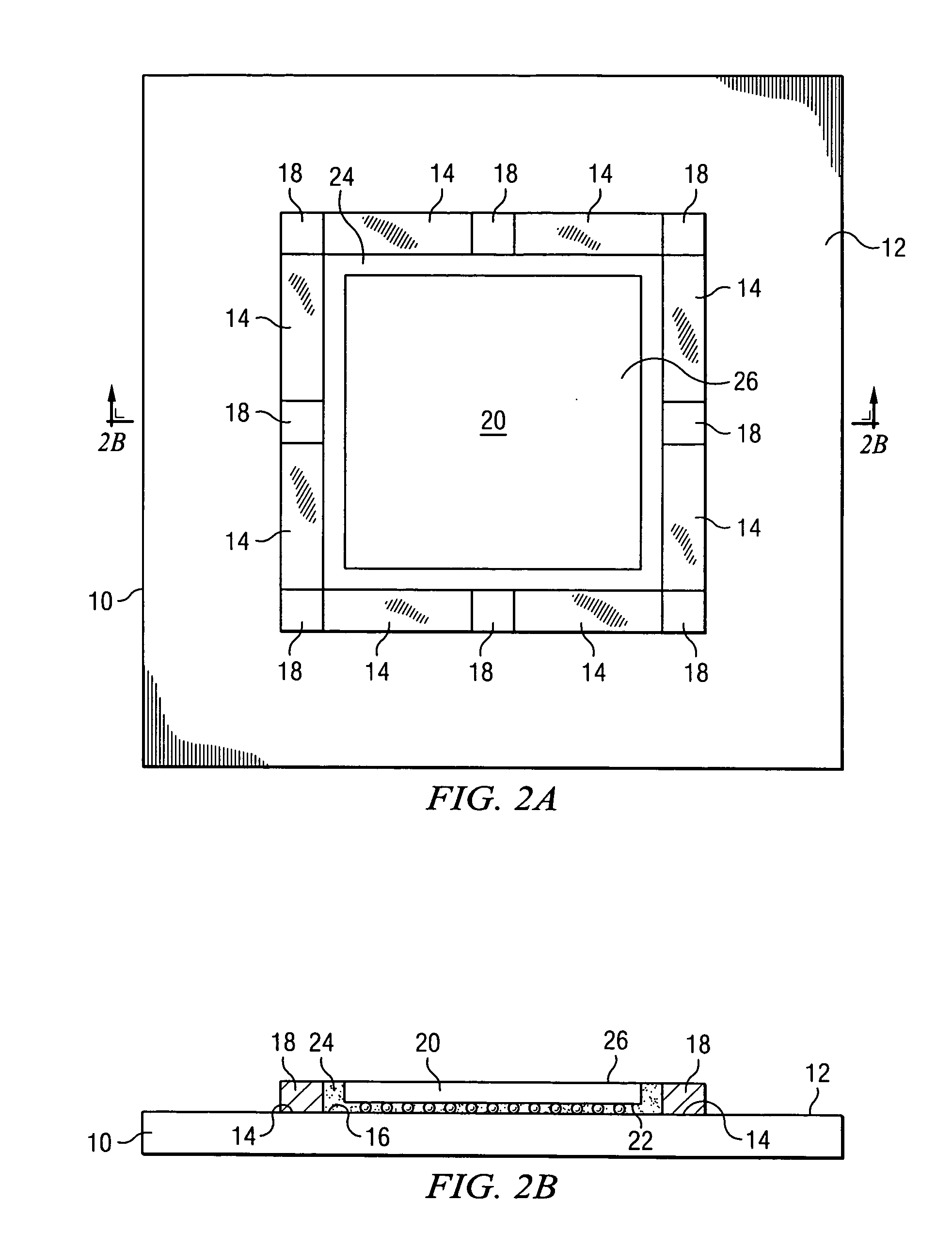
[0023] In general, the invention provides thermally enhanced BGAs and methods for their fabrication with a backside heat spreader and a ground ring suitable for operably coupling to either the frontside or backside, or both, of an IC chip, preferably a flip-chip. As further described below, the approach of the invention includes the fabrication of a ground ring on the surface of a BGA substrate prepared for receiving the frontside of a chip, and the attachment of a heat spreader with a corresponding ground ring at the backside of the chip. The chip is affixed to a mounting site on the substrate, and is underfilled with a non-conductive material. The heat spreader is attached to the backside of the chip with a conductive material such as epoxy or solder, and cured. A conductive material is injected between the heat spreader and substrate, electrically coupling the heat spreader and substrate ground rings. Thus, the backside of the chip may be electrically connected to ground in addit...


PUM


Abstract

The invention provides thermally enhanced BGAs and methods for their fabrication with a ground ring suitable for operably coupling to either the frontside or backside, or both, of an IC chip mounted on a substrate. The methods and devices of the invention disclosed include the fabrication of a ground ring on the surface of a BGA substrate prepared for receiving the frontside of the chip. A heat spreader has ground ring corresponding to substrate round ring and is attached at the backside of the chip with a conductive material. A conductive material is interposed between the heat spreader and substrate ground rings, electrically coupling them. Thus, the backside of the chip may be electrically connected to the ground ring as well as, or instead of, the frontside.

Description

TECHNICAL FIELD [0001] The invention relates to electronic semiconductor devices and manufacturing. More particularly, the invention relates to surface-mount BGA-packaged flip-chip semiconductor devices and to methods for the manufacture of the same. BACKGROUND OF THE INVENTION [0002] The ball grid array (BGA) is a well-known type of surface-mount package that utilizes an array of metallic bumps or nodules, often denominated “solder balls,” as means for providing external electrical connections. The solder balls are attached to a laminated substrate at the bottom side of the package. The die, or integrated circuit (IC) chip of the BGA is commonly connected to the substrate by flip-chip connections. The term “flip-chip” refers to a semiconductor chip that can be mounted directly onto a substrate or PCB in a “face-down” orientation. Electrical connections are completed through conductive bumps built on the surface of the chip, thus the mounting process is frontside down. Because flip-...

Claims


Application Information

Patent Timeline
Patent Type & Authority Applications(United States)
IPC IPC(8): H01L23/34
CPCH01L21/563H01L2924/3025H01L23/36H01L23/50H01L2224/73203H01L2924/01057H01L2924/18161H01L2224/16225H01L2224/32225H01L2224/73204H01L2924/15311H01L23/24H01L2224/73253H01L2224/32245H01L2924/00
Inventor HAGA, CHRISSWANSON, LELAND
Owner TEXAS INSTR INC
Why Eureka
Try Eureka