Thermally Enhanced BGA Packages and Methods

a technology of bga packages and semiconductors, applied in semiconductor devices, semiconductor/solid-state device details, electrical apparatus, etc., can solve the problems of stress at the connecting solder ball, the bga package as a whole tends to thermally expand and contract, and the heat concentration of excess heat generated during circuit operation, etc., to achieve the effect of improving the thermal path and being easily integrated into the typical end user system

Inactive Publication Date: 2008-04-10
TEXAS INSTR INC
View PDF16 Cites 12 Cited by
  • Summary
  • Abstract
  • Description
  • Claims
  • Application Information

AI Technical Summary

Benefits of technology

[0013]The invention has advantages including but not limited to providing an improved thermal path for the egress of heat from a packaged semiconductor device in a package format which is easily integrated into typical end user systems. This and other features, advantages, and benefits of the present invention can be understood by one of ordinary skill in the arts upon careful consideration of the detailed description of representative embodiments of the invention in connection with the accompanying drawings.

Problems solved by technology

All packages have drawbacks, however, and the BGA is no exception.
The high density of the BGA which makes it desirable for many applications can lead to a concentration of excess heat generated during operation of the circuitry.
Due to the changes in temperature, the BGA package as a whole tends to thermally expand and contract.
However, since in many cases the thermal expansion behavior of the package, its internal components, e.g., chip, substrate, and PCB differ, stresses can occur at the connecting solder balls, or within the layers of the PCB, or among the components of the package.
This is typically a relatively poor heat path due to inherent heat resistance of the encapsulant material, although heat conduction may sometimes be improved by the use of heat-conductive mold compound material, the inclusion of a heat spreader or external heat sink, or by using a thin mold cap.
This can be a better heat path than through the encapsulant, particularly in packages with thick substrates, but in some instances may be insufficient.
These improvements are necessarily limited by the available area and are not sufficient in all cases however, leaving a need for thermally enhanced BGA packages.
This technology, however, has its own problems.
The primary problem is related to assembly of the package onto the PCB.
Manufacturing and interposing the heat spreader between the semiconductor chip and the PCB complicates production procedures, resulting in increased costs.
Also, there are various challenges to attaching the heat spreader to the substrate, and in sealing the junctions between the heat spreader, chip, and substrate.
Also, due to rigid attachment of the heat spreader to the PCB, there may be a degradation in reliability of the device due to the effects of thermally-induced stresses.
Additionally, although it is desirable to make the heat spreader large in order to dissipate heat more effectively, larger sizes can lead to further problems such as increased susceptibility to warpage.

Method used


Image

  • Thermally Enhanced BGA Packages and Methods
  • Thermally Enhanced BGA Packages and Methods
  • Thermally Enhanced BGA Packages and Methods

Examples


Embodiment Construction

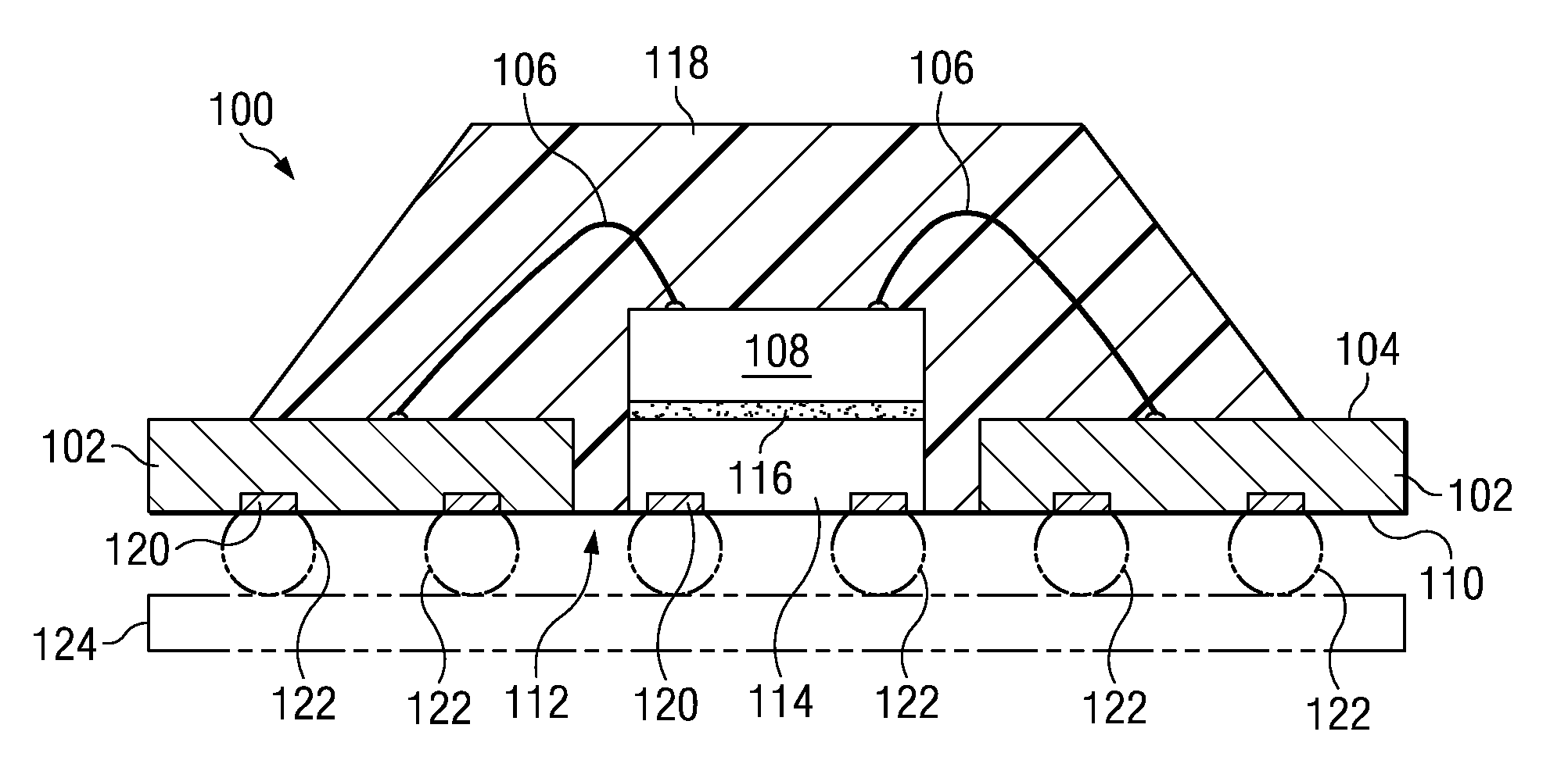
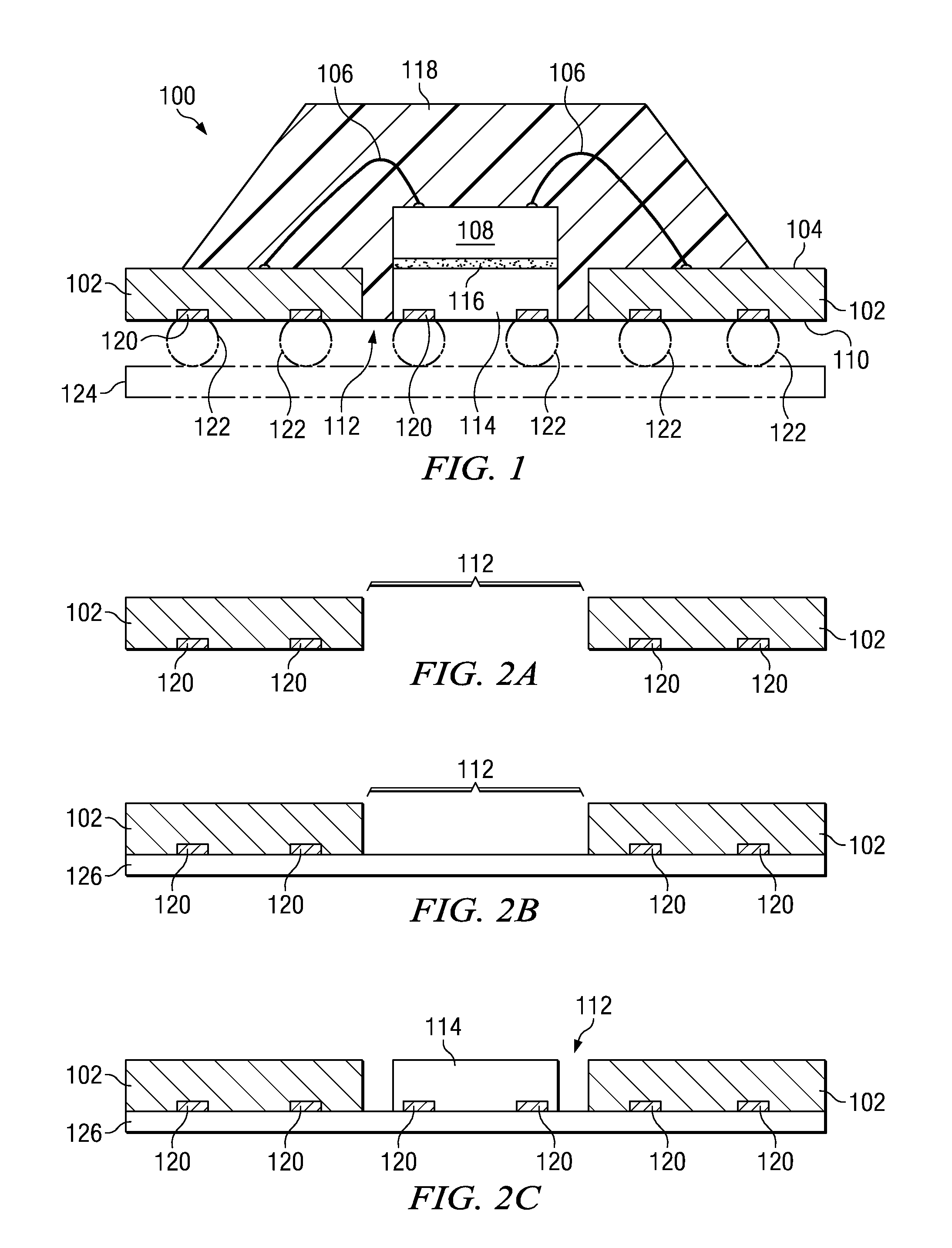
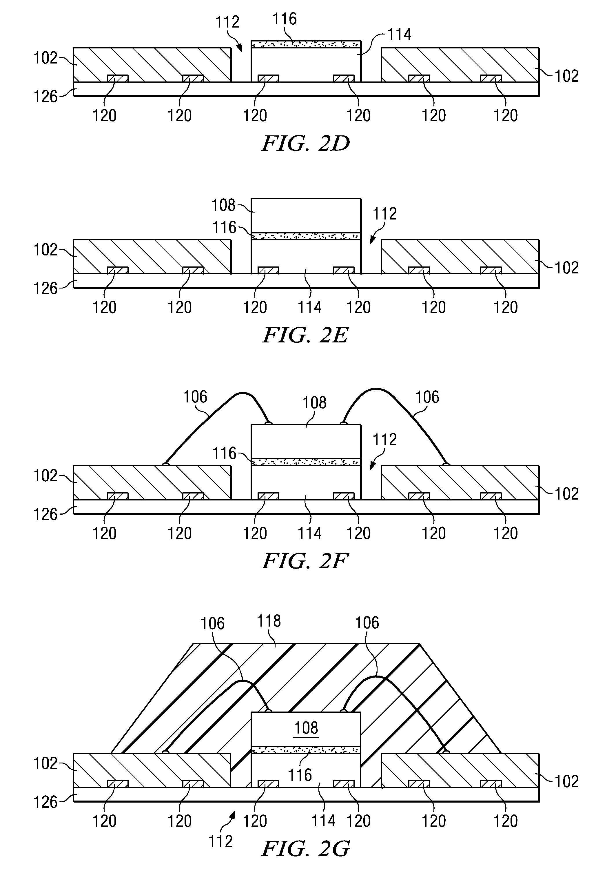
[0027]In general, the invention enhances the thermal path from the IC to the bottom of the BGA package, e.g., to an attached PCB, with a much higher-conductivity path by providing a heat channel element made from material favorable for the conduction of heat, preferably silicon. The heat channel element is configured to accept solder ball attachment on its bottom surface, preferably masked and patterned in the manner of the substrate, thus providing a good thermal path from the IC to the PCB. The devices and methods of the invention may be implemented using cost-effective modifications to standard assembly processes.

[0028]Now referring primarily to FIG. 1, an example of a preferred embodiment of a BGA package 100 according to the invention is shown in a cut-away side view. A semiconductor substrate 102 provides the foundation of the package 100 as generally understood in the art. The substrate 102 carries interconnecting circuitry (not shown) and the top surface 104 of the substrate...


PUM


Abstract

BGA packages have thermal properties which are enhanced by a heat channel through the substrate. Solder ball attachment points are provided at the surface of the heat channel for receiving solder balls. A BGA includes an IC operably coupled to a substrate having a top surface for receiving the IC and a bottom surface defining the perimeter of the package bottom. An encapsulant encloses the IC and at least a portion of the top surface of the substrate, defining the top and sides of the package. The substrate includes a heat channel aperture for receiving heat channel having a surface proximal to the IC and having a patterned opposing surface defining at least an interior portion of the package bottom and coupling to solder balls. Methods for assembling packages are disclosed in which a substrate is provided with a heat channel aperture and the heat channel is placed therein.

Description

TECHNICAL FIELD[0001]The invention relates to electronic semiconductor devices and manufacturing. More particularly, the invention relates to surface-mount BGA-packaged semiconductor devices and to methods for the manufacture of the same.BACKGROUND OF THE INVENTION[0002]The ball grid array (BGA) is a well-known type of surface-mount package that utilizes an array of metallic nodules, often denominated “solder balls” although they are not necessarily spherical, as means for providing external electrical connections. The solder balls are attached to a layered substrate at the bottom side of the package. The die, or integrated circuit (IC) chip of the BGA is connected to the substrate commonly either by wirebond or flip-chip connections. The layered substrate of a BGA has internal conductive paths that electrically connect the chip bonds to the ball array. This substrate is typically encapsulated with a plastic mold or glob top to form the top of the package. Typically a BGA, or PBGA (...

Claims


Application Information

Patent Timeline
Patent Type & Authority Applications(United States)
IPC IPC(8): H01L23/34H01L21/00
CPCH01L23/13H01L2924/10253H01L23/4334H01L2224/48091H01L2224/48227H01L2224/48465H01L2224/73265H01L2924/01029H01L23/3128H01L2224/92247H01L2924/15311H01L2224/32145H01L24/48H01L2924/00014H01L2924/00H01L2224/32225H01L2924/00012H01L24/73H01L2924/14H01L2924/181H01L2224/45099H01L2224/45015H01L2924/207
Inventor ROMIG, MATTHEW D.MATHEW, THOMAS
Owner TEXAS INSTR INC
Why Eureka
Try Eureka