System and method for designing a common centroid layout for an integrated circuit

a technology of integrated circuits and layouts, applied in the direction of program control, instruments, total factory control, etc., can solve the problems of affecting tolerances and/or creating mismatches within the ic chip, and affecting the design quality of the integrated circuit. manual creation of a common centroid layout for the ic chip can be burdensome and time-consuming,

Active Publication Date: 2007-12-20
ADTRAN
View PDF8 Cites 171 Cited by
  • Summary
  • Abstract
  • Description
  • Claims
  • Application Information

AI Technical Summary

Problems solved by technology

Imperfections in manufacturing of an integrated circuit (IC) chip may result in some parameters varying either linearly or non-linearly along the surface of the chip.
Such variations may adversely affect tolerances and / or create mismatches within the IC chip.
To achieve this affect, the transistors of a current mirror are typically designed to have the same characteristics, but variations in the manufacturing process may cause a mismatch between transistors, thereby causing the output current to slightly differ from the input current.
Manually creating a common centroid layout for an IC chip can be burdensome and time consuming.
Unfortunately, automating this process has proven difficult.
Generally, previous systems for generating common centroid layout designs have been complex and capable of successfully handling only a limited number of types.
Further, many layout designers have been reluctant to use such systems because they do not trust these systems to generate an accurate common centroid layout for each object using complex and computationally expensive algorithms.
Accordingly, previous systems for automating creation of common centroid layout designs have, in general, achieved only limited success.

Method used


Image

  • System and method for designing a common centroid layout for an integrated circuit
  • System and method for designing a common centroid layout for an integrated circuit
  • System and method for designing a common centroid layout for an integrated circuit

Examples


Embodiment Construction

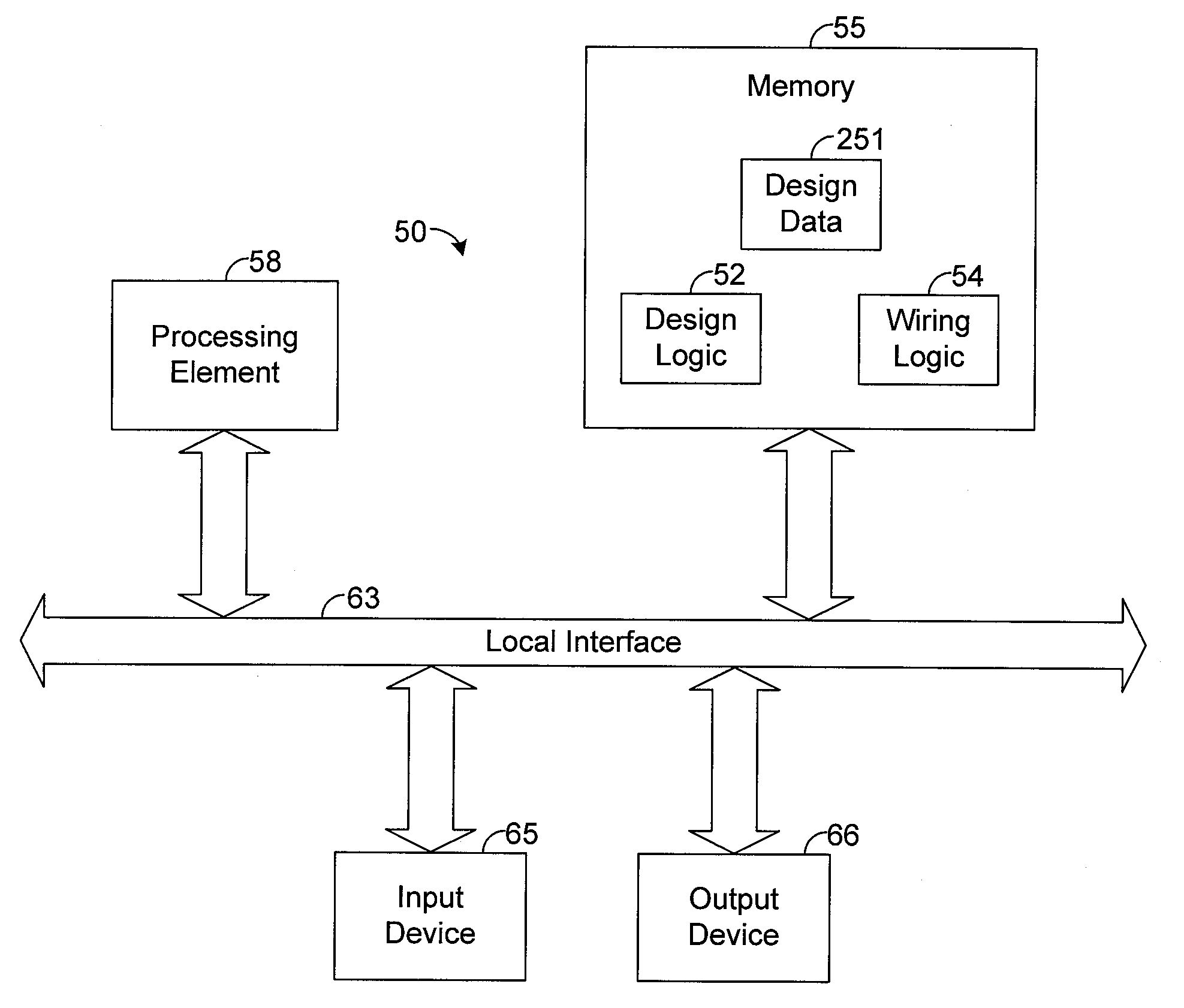
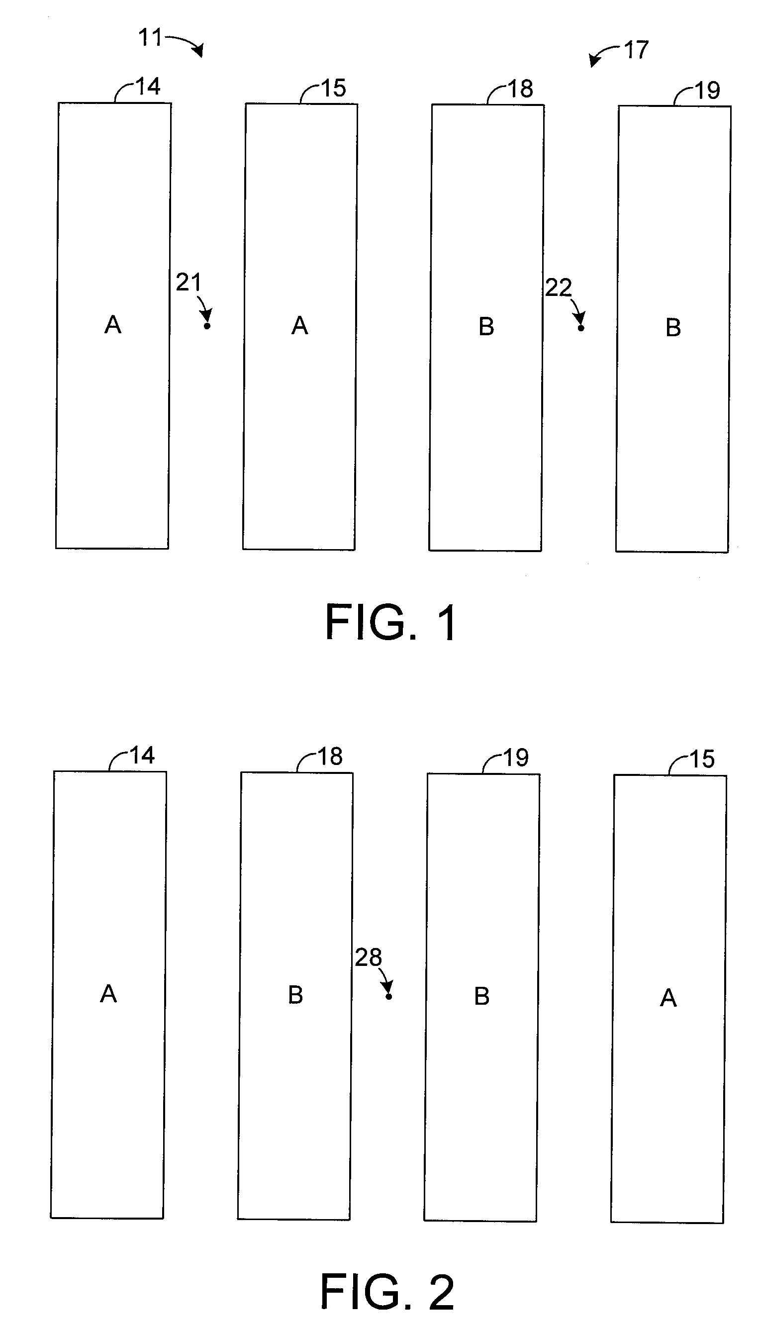
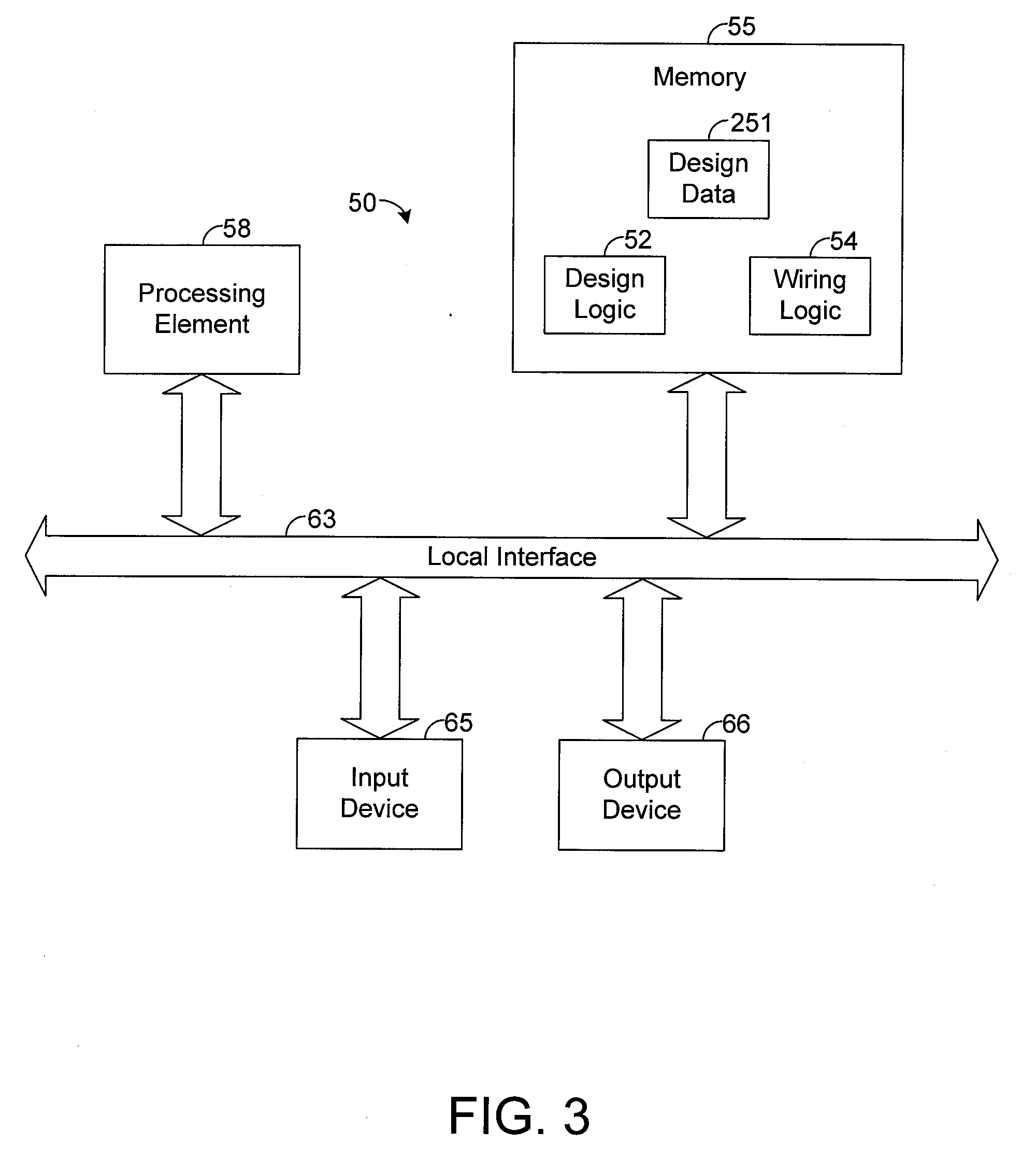
[0028] The present disclosure generally pertains to systems and methods for automatically generating common centroid layout designs for integrated circuits (ICs). A system for designing a common centroid layout in accordance with an exemplary embodiment of the present disclosure receives various inputs, such as the number of devices and size of each device, pertaining to the circuit design for at least one IC object. Based on such inputs, the system calculates a common centroid unit, which represents an array of device segments. (The number of segments for each device within the common centroid unit is selected based on the respective sizes of the devices.) The common centroid unit is then tiled to automatically define the complete layout for the object. The system selects an algorithm for tiling the common centroid unit based on the size of this unit such that, upon completion of the tiling process, all of the devices have a common centroid (i.e., have a center of mass located at t...


PUM


Abstract

An exemplary common centroid layout design system receives various inputs about an integrated circuit (IC) design. Based on such inputs, the system calculates a common centroid unit, which represents an array of segments of each device in the IC design. The number of segments for each device within the common centroid unit is selected based on the respective sizes of the devices. The common centroid unit is then tiled to automatically define the complete layout for the IC object. The system selects an algorithm for tiling the common centroid unit based on the size of such unit such that, upon completion of the tiling process, all of the devices have a common centroid. In other words, the system selects an algorithm for tiling such that a common centroid layout design is generated. Using the common centroid layout design, the IC object can be manufactured so that it is immune to linear process gradients and more resistant to non-linear gradients relative to ICs that do not have a common centroid layout design.

Description

CROSS REFERENCE TO RELATED APPLICATIONS [0001] This application claims priority to U.S. Provisional Patent Application No. 60 / 815,028, entitled “Automatic Generation of Common-Centroid Arrays,” and filed on Jun. 20, 2006, which is incorporated herein by reference. This application also claims priority to U.S. Provisional Patent Application No. 60 / 838,084, entitled “A Systematic Method for Wiring Common-Centroid Cells,” and filed on Aug. 16, 2006, which is incorporated herein by reference.RELATED ART [0002] Imperfections in manufacturing of an integrated circuit (IC) chip may result in some parameters varying either linearly or non-linearly along the surface of the chip. Such variations may adversely affect tolerances and / or create mismatches within the IC chip. As an example, it is well-known that, for a unity-gain current mirror, the input current ideally should equal the output current. To achieve this affect, the transistors of a current mirror are typically designed to have the ...

Claims


Application Information

Patent Timeline
Patent Type & Authority Applications(United States)
IPC IPC(8): G06F17/50
CPCG06F2217/12G06F17/5068G06F30/39G06F2119/18Y02P90/02
Inventor BOWEN, C. TREVOR
Owner ADTRAN
Why Eureka
Try Eureka