Film formation apparatus and method for using the same

Active Publication Date: 2008-01-03
TOKYO ELECTRON LTD
View PDF5 Cites 14 Cited by
  • Summary
  • Abstract
  • Description
  • Claims
  • Application Information

AI Technical Summary

Benefits of technology

[0009] An object of the present invention is to provide a film formation apparatus for a semiconductor process and a method for using t

Problems solved by technology

The particles may drop on semiconductor wafers, and reduce the yield of semiconductor devices to be fabricated.
Furth

Method used


Image

  • Film formation apparatus and method for using the same
  • Film formation apparatus and method for using the same
  • Film formation apparatus and method for using the same

Examples


Example

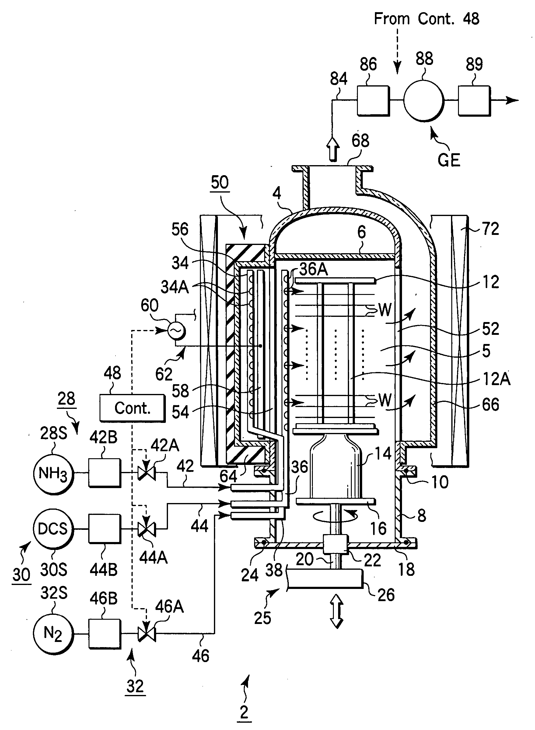
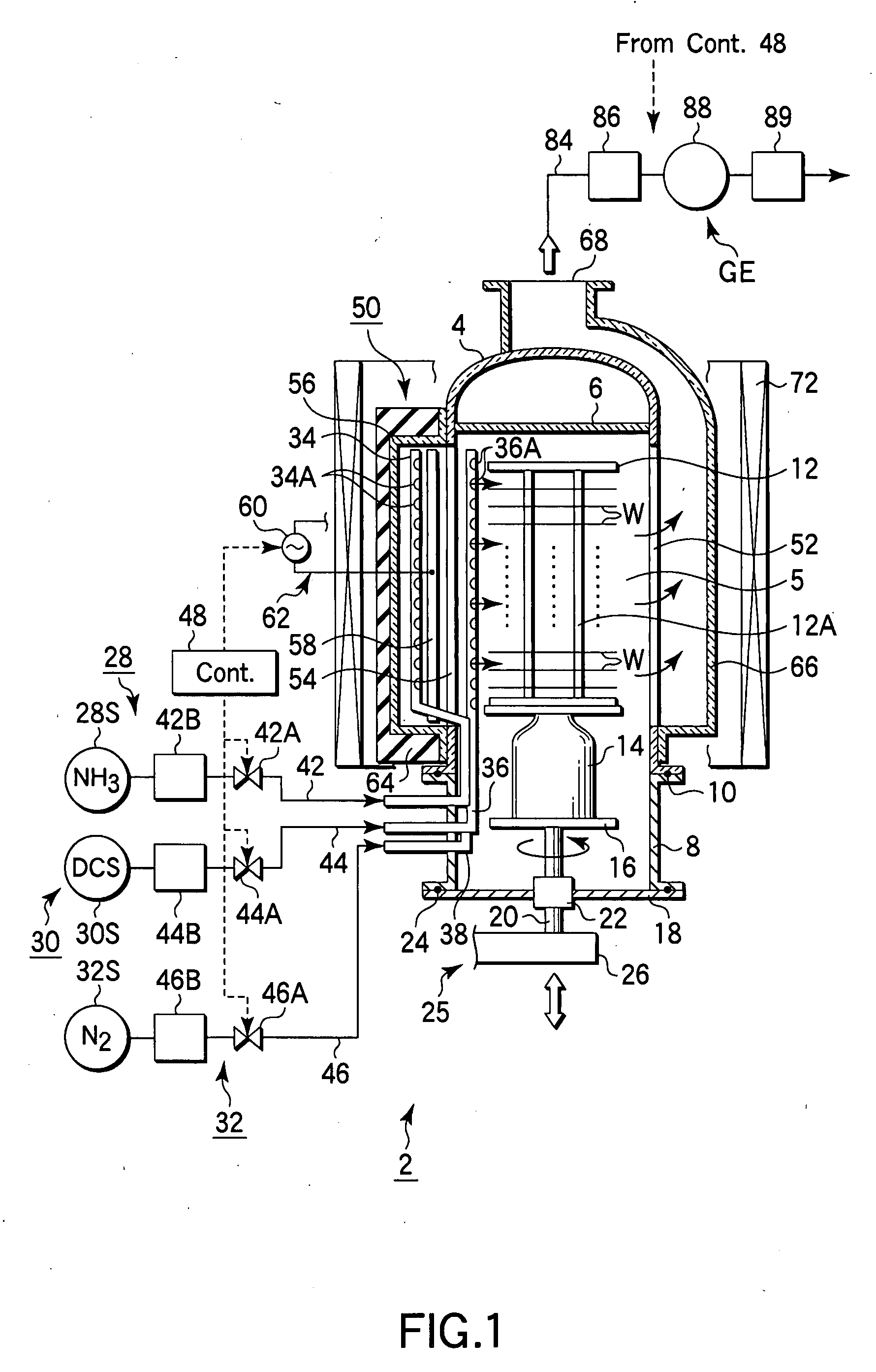
[0045] In the process of developing the present invention, the inventors studied problems caused in the techniques disclosed in Patent Documents 1 and 2 described above. As a result, the inventors have arrived at the findings given below.

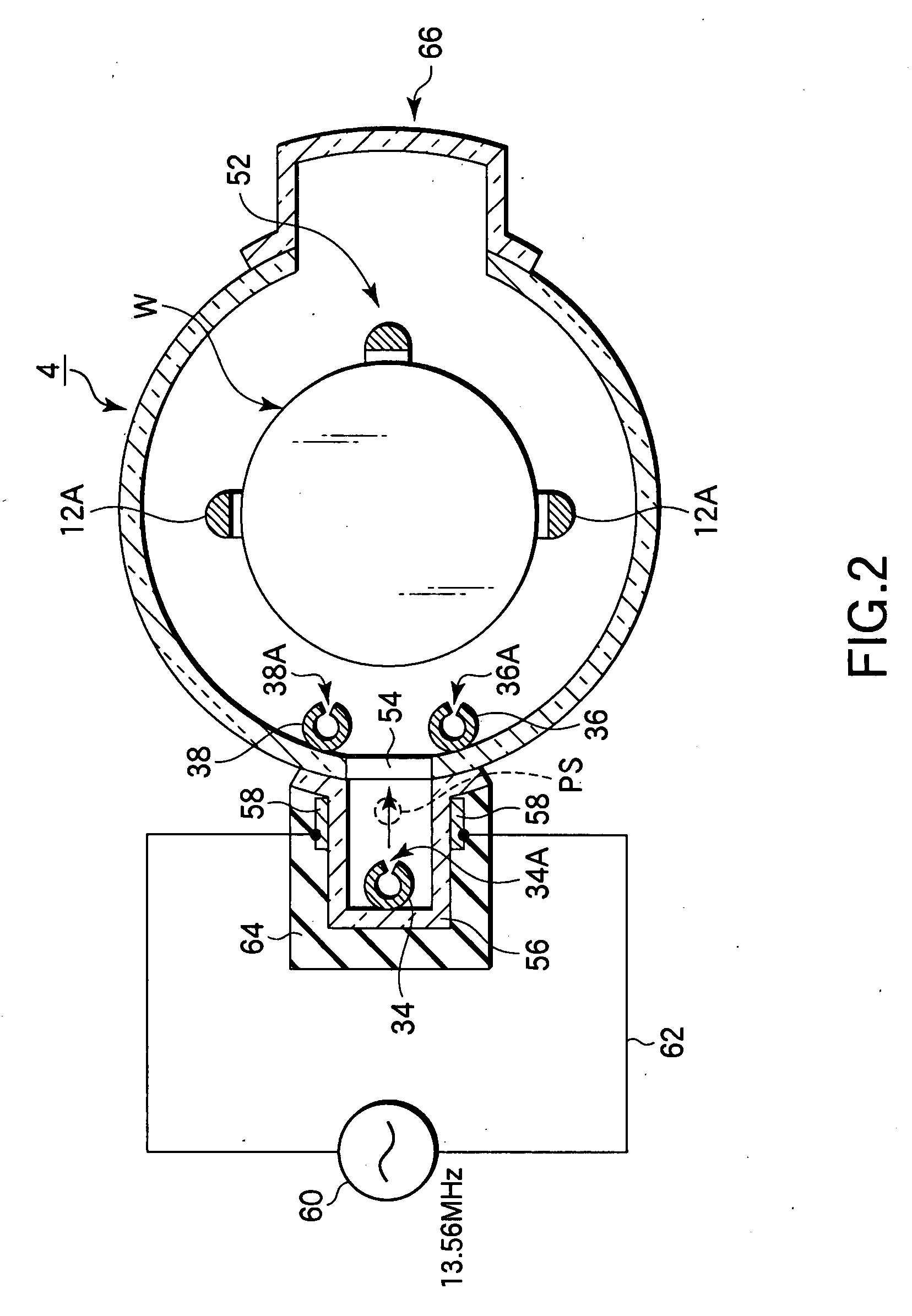
[0046] Specifically, where the purge process of Patent Document 1 arranged to cool the interior of the process container was applied to the film formation method of Patent Document 2 utilizing plasma assistance, an expected decrease in the number of particles was not attained in the film formation process. By studying this problem, it has been found that the main cause resides in that a certain condition within the process container is less uniform due to a factor peculiar to the film formation method utilizing plasma assistance. Specifically, since the activation level of ammonia (NH3) is optimized for a process field in which wafers are placed, radicals have been deactivated or decreased at some areas around the process field, such as a position ...


PUM

PropertyMeasurementUnit
Temperatureaaaaaaaaaa

Abstract

A method for using a film formation apparatus includes performing film formation of a product film selected from the group consisting of a silicon nitride film and a silicon oxynitride film on a target substrate within a reaction chamber of the film formation apparatus; and unloading the target substrate from the reaction chamber. Thereafter, the method includes first heating an inner surface of the reaction chamber at a post process temperature while supplying a post process gas for nitridation into the reaction chamber, thereby performing nitridation of a by-product film deposited on the inner surface of the reaction chamber; then rapidly cooling the inner surface of the reaction chamber, thereby cracking the by-product film by a thermal stress; and then forcibly exhausting gas from inside the reaction chamber to carry the by-product film, thus peeled off from the inner surface.

Description

BACKGROUND OF THE INVENTION [0001] 1. Field of the Invention [0002] The present invention relates to a film formation apparatus for a semiconductor process for forming a film on a target substrate, such as a semiconductor wafer, and also to a method for using the apparatus. The term “semiconductor process” used herein includes various kinds of processes which are performed to manufacture a semiconductor device or a structure having wiring layers, electrodes, and the like to be connected to a semiconductor device, on a target substrate, such as a semiconductor wafer or a glass substrate used for an FPD (Flat Panel Display), e.g., an LCD (Liquid Crystal Display), by forming semiconductor layers, insulating layers, and conductive layers in predetermined patterns on the target substrate. [0003] 2. Description of the Related Art [0004] In the process of manufacturing semiconductor devices, a process is performed for forming a silicon nitride film on the surface of a target substrate, suc...

Claims


Application Information

Patent Timeline
IPC IPC(8): C23C16/00B05C11/00
CPCC23C16/4404Y10S438/905H01L21/67109C23C16/4405H01L21/31
Inventor NODERA, NOBUTAKEHASEBE, KAZUHIDEYAMAMOTO, KAZUYA
Owner TOKYO ELECTRON LTD
Why Eureka
Try Eureka