Phase change memory device and method for manufacturing the same

a phase change memory and memory device technology, applied in the direction of bulk negative resistance effect devices, semiconductor devices, electrical equipment, etc., can solve the problems of poor sensing margin and high integration difficulty of phase change memory devices, and achieve the effect of quick cooling

Inactive Publication Date: 2009-02-12
SK HYNIX INC
View PDF4 Cites 50 Cited by
  • Summary
  • Abstract
  • Description
  • Claims
  • Application Information

AI Technical Summary

Benefits of technology

[0014]The present invention provides a phase change memory device which allows the heat generated by the reset current transmitted to a phase change layer to be quickly cooled and a method for manufacturing the same.

Problems solved by technology

When the surface area of the electrode is increased, high levels of integration become difficult.
All of these factors present difficulties when attempting to accomplish high levels of integration.
Accordingly, in a conventional phase change memory device, when the heat transferred from the heater to the phase change layer is not quickly cooled, the phase change layer will not have a stable reset resistance, resulting in a poor sensing margin in the phase change memory device, and thus concerns emerge regarding the reliability of the conventional phase change memory device.

Method used


Image

  • Phase change memory device and method for manufacturing the same
  • Phase change memory device and method for manufacturing the same
  • Phase change memory device and method for manufacturing the same

Examples


Embodiment Construction

[0062]Hereafter, specific embodiments of the present invention will be described in detail with reference to the attached drawings.

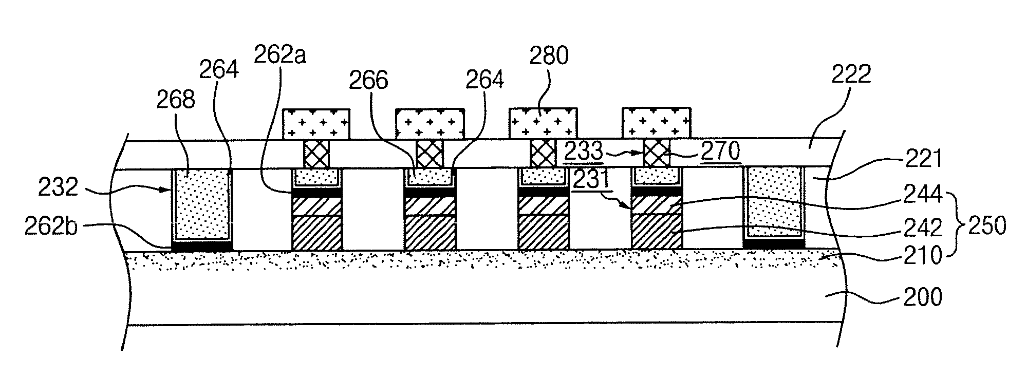
[0063]FIG. 2 is a cross-sectional view showing a phase change memory device in accordance with an embodiment of the present invention.

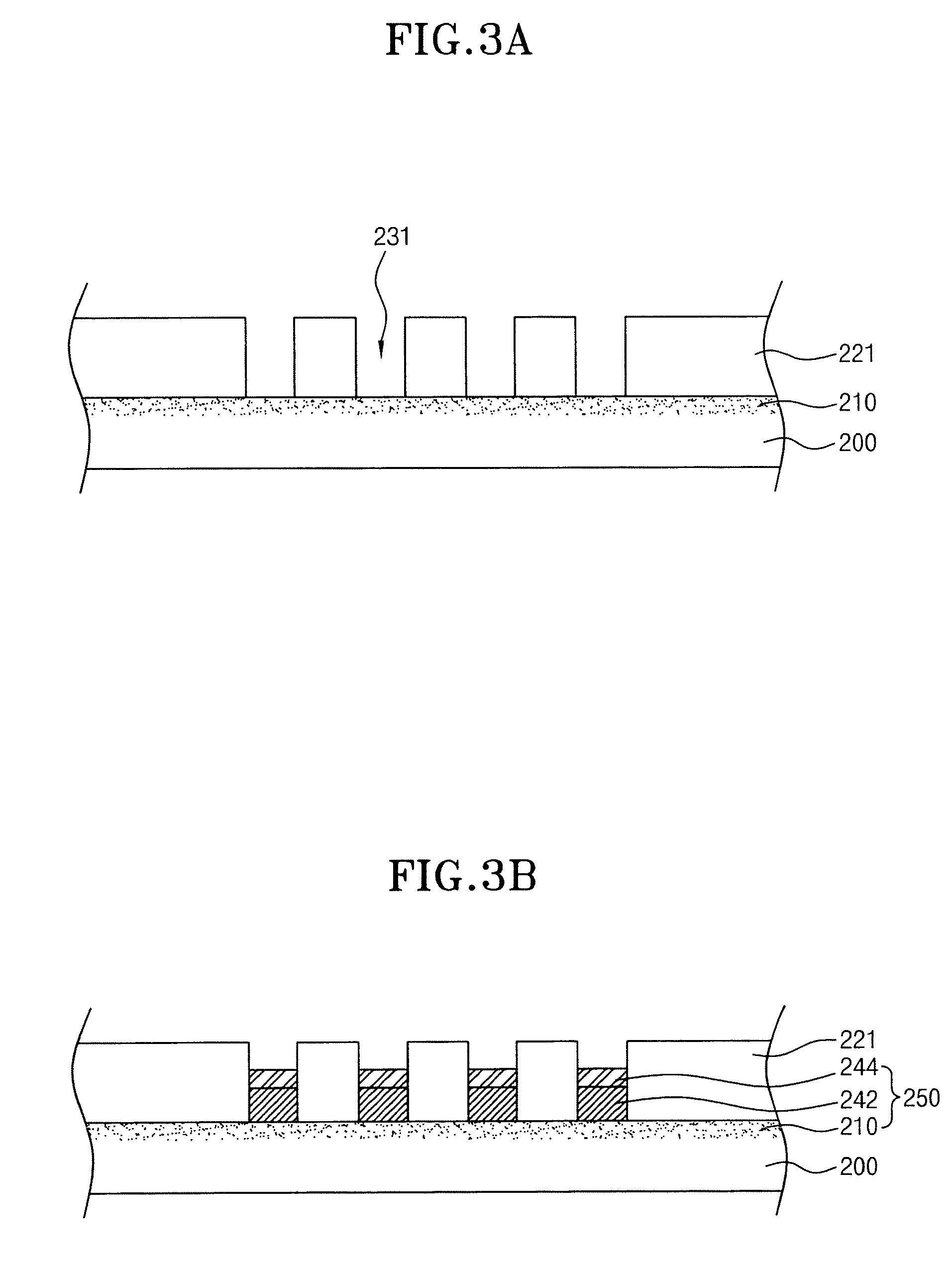
[0064]Referring to FIG. 2, a silicon substrate 200 is prepared. The silicon substrate 200 has a bar-type active region that comprises a plurality of phase change cell areas. An N-type impurity region 210 is formed in the surface of the active region of the silicon substrate 200. A first insulation layer 221 is formed on the silicon substrate 200 including the N-type impurity region 210. First contact holes 231 are defined in portions of the first insulation layer 221 corresponding to respective phase change cell areas. Second contact holes 232 are defined in portions of the first insulation layer 221 on both sides of the plurality of phase change cell areas to expose the N-type impurity region 210 formed in the surface of ...


PUM


Abstract

A phase change memory device includes a silicon substrate having a bar-type active region and an N-type impurity region formed in a surface of the active region. A first insulation layer is formed on the silicon substrate, and the first insulation layer includes a plurality of first contact holes and second contact holes. PN diodes are formed in the first contact holes. Heat sinks are formed in the first contact holes on the PN diodes, and contact plugs fill the second contact holes. A second insulation layer having third contact holes is formed on the first insulation layer. Heaters fill the third contact holes. A stack pattern of a phase change layer and a top electrode is formed to contact the heaters. The heat sink quickly cools heat transferred from the heater to the phase change layer.

Description

CROSS-REFERENCE TO RELATED APPLICATIONS[0001]The present application claims priorities to Korean patent application numbers 10-2007-0080302 filed on Aug. 9, 2007 and 10-2008-0025443 filed on Mar. 19, 2008, which are incorporated herein by reference in their entireties.BACKGROUND OF THE INVENTION[0002]The present invention relates to a phase change memory device and a method for manufacturing the same, and more particularly, to a phase change memory device which enables manufacturing of a highly integrated phase change memory device having stable reset resistance and a method for manufacturing the same.[0003]Memory devices are typically classified into two categories: volatile random access memory (RAM), which loses inputted information when power is interrupted; and non-volatile read-only memory (ROM), which can continuously maintain the stored state of inputted information even when power is interrupted. Examples of volatile RAM include dynamic RAM (DRAM) and static RAM (SRAM), and...

Claims


Application Information

Patent Timeline
Patent Type & Authority Applications(United States)
IPC IPC(8): H01L45/00
CPCH01L27/2409H01L45/06H01L45/144H01L45/126H01L45/128H01L45/1233H10B63/20H10N70/8413H10N70/861H10N70/231H10N70/8828H10N70/826
Inventor CHANG, HEON YONGKIM, MYOUNG SUBDO, GAP SOK
Owner SK HYNIX INC
Why Eureka
Try Eureka