Method of forming a thin film by plasma CVD of a silicon-containing source gas

a source gas and plasma technology, applied in the field of thin film forming, can solve the problems of low mechanical strength of films compared with teos oxide films, low mechanical strength of films, and high mechanical strength of films having spin-on type low-k films, so as to reduce plasma damage

Active Publication Date: 2007-06-12
ASM JAPAN
View PDF6 Cites 4 Cited by
  • Summary
  • Abstract
  • Description
  • Claims
  • Application Information

AI Technical Summary

Benefits of technology

[0011]Consequently, in an aspect, an object of the present invention is to provide a method for forming a thin film, which reduces plasma damage.
[0012]In another aspect, an object of the present invention is to provide a method for forming a thin film, which improves adhesion between thin films.
[0013]In still another aspect, an object of the present invention is to provide a method for forming a thin film, which inhibits particle contamination caused by silicon-containing source gases.
[0014]In yet another aspect, an object of the present invention is to provide a method for forming a thin film, which inhibits the occurrence of sticking.
[0032]In at least one embodiment of the present invention, it is possible to reduce the plasma damage occurrence when the applying of the radio-frequency power is stopped. Further, in at least one embodiment of the present invention, because adhesion of films having low mechanical strength such as low-k films and ULK films to thin films formed in the subsequent process can be improved, exfoliation and scratches caused in a CMP (Chemical Mechanical Polishing) process can be prevented. Additionally, in at least one embodiment of the present invention, because of low rest potential, the occurrence of sticking can be prevented. Furthermore, in at least one embodiment of the present invention, particle contamination caused by residual silicon-containing source gas components can be controlled.

Problems solved by technology

Because the low-k films contain carbon in oxide film bonding, the films have a drawback of low mechanical strength as compared with TEOS oxide films.
This mechanical strength brittleness poses a problem in the Damascene process.
In such cases, adhesion among plasma type low-k films having low mechanical strength, SiO or SiC films having high mechanical strength and spin-on type low-k films becomes a problem.
In plasma CVD, plasma damage has been a problem.
If the leakage current exceeds a certain value, a gate insulation film of a semiconductor apparatus is deteriorated or destroyed, thereby lowering a semiconductor apparatus yield rate.
These methods, however, have problems of process-gas resistance, plasma resistance and heat resistance of anodic oxide films and of exfoliation of precoat films; in order to solve these problems, methods using alloy materials excellent in corrosion resistance and resistance properties were proposed (For example, Japanese Patent Laid-open No. 1999-229185).
This method, however, has a problem because changing the process conditions changes film properties.
Conversely, if the plasma amount applied is increased, sheath voltage is increased and damage on a semiconductor substrate occurs.

Method used


Image

  • Method of forming a thin film by plasma CVD of a silicon-containing source gas
  • Method of forming a thin film by plasma CVD of a silicon-containing source gas
  • Method of forming a thin film by plasma CVD of a silicon-containing source gas

Examples


examples

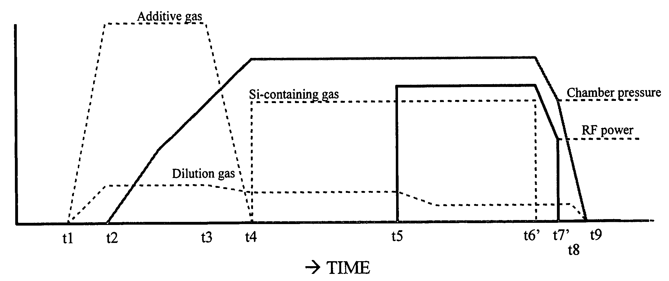
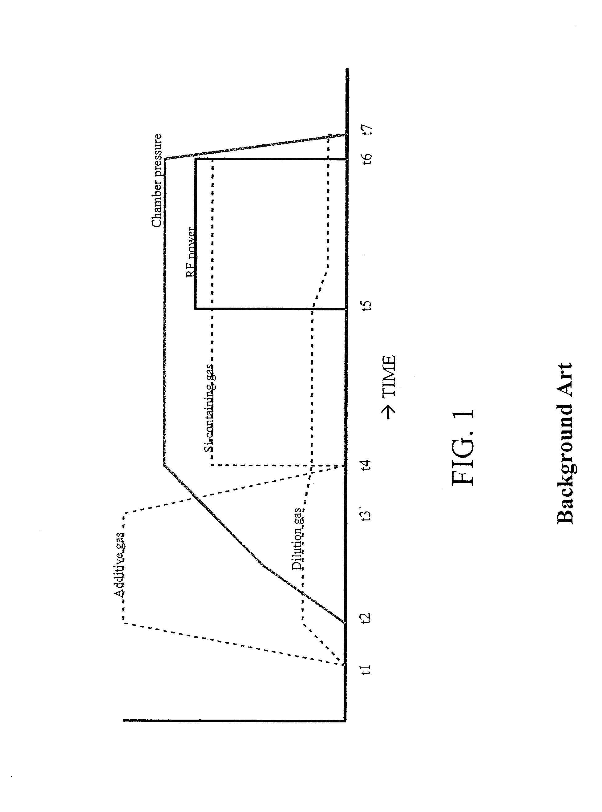
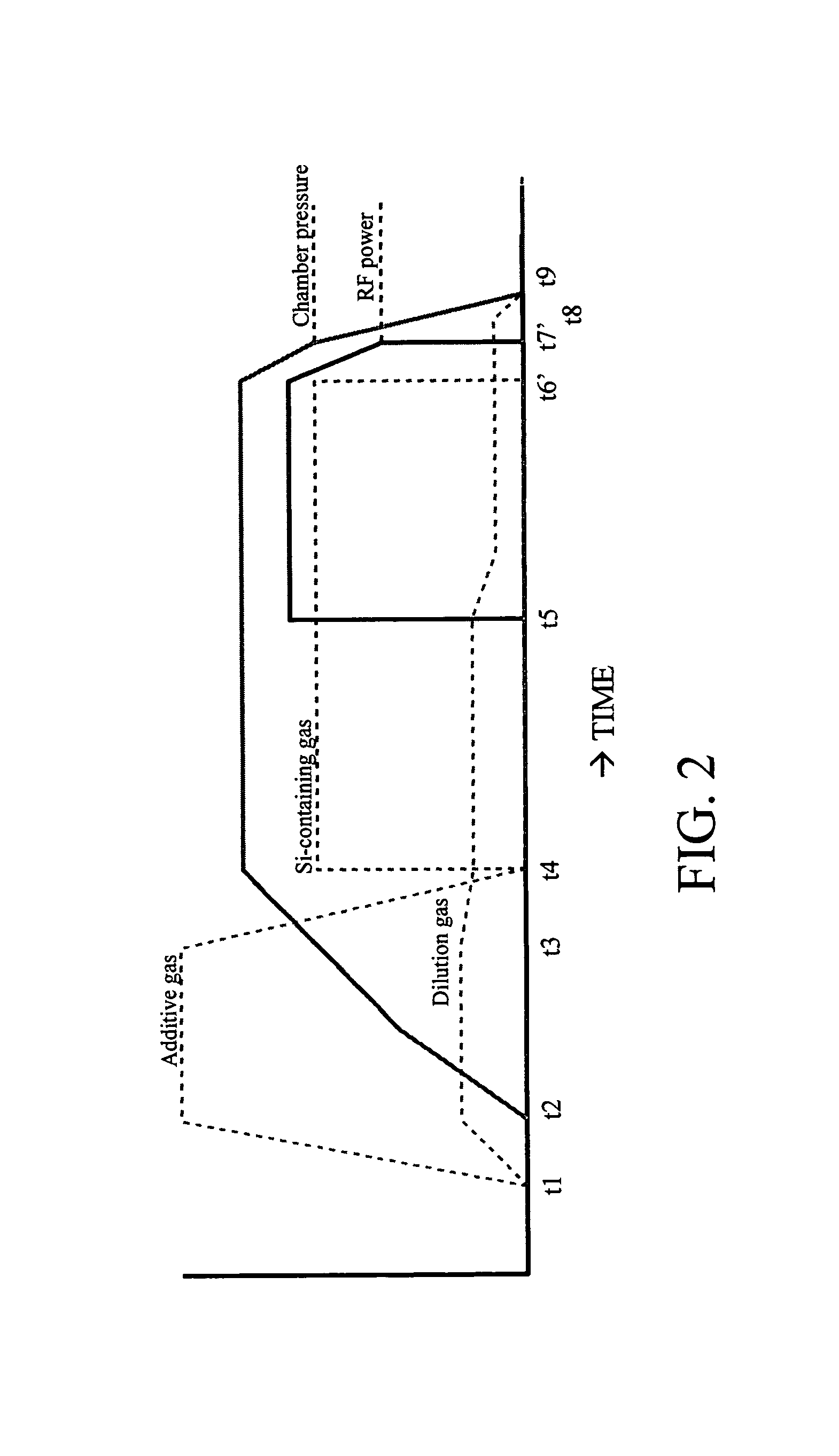
[0057]Evaluation experiments of insulation films formed using the method according to embodiments of the present invention were conducted and the results are described below. Table 1 shows the measurement results of surface potential, interface state density and flat band voltage of silicon-containing insulation thin films (ULK films formed using 1,3 dimethoxytetramethyldisiloxane (DMOTMDS) as a source gas, O2 and isopropyl alcohol as additive gases and He as a dilution gas) formed using the comparative sequence and the sequence according to the above-mentioned embodiment of the present invention; Table 2 shows the measurement results of surface potential, interface state density and flat band voltage of silicon-containing insulation thin films (low-k films formed using dimethyldimethoxysilane as a source gas and He as a dilution gas) formed using the comparative sequence and the sequence according to the embodiment of the present invention.

[0058]

TABLE 1UniformityMax.Min.Mean(%)Rang...


PUM

PropertyMeasurementUnit
timeaaaaaaaaaa
temperatureaaaaaaaaaa
pressureaaaaaaaaaa

Abstract

A method for forming a thin film includes: supplying an additive gas, a dilution gas, and a silicon-containing source gas into a reaction chamber wherein a substrate is placed; forming a thin film on the substrate by plasma CVD under a given pressure with a given intensity of radio-frequency (RF) power from a first point in time to a second point in time; at the second point in time, stopping the supply of the silicon-containing source gas; and at the second point in time, beginning reducing but not stopping the RF power, and beginning reducing the pressure, wherein the reduction of the RF power and the reduction of the pressure are synchronized up to a third point in time.

Description

BACKGROUND OF THE INVENTION[0001]1. Field of the Invention[0002]The present invention generally relates to a method for forming a thin film in a semiconductor device circuit manufacturing process; and particularly to a method for forming a thin film, which reduces plasma damage in plasma CVD.[0003]2. Description of the Related Art[0004]Conventionally, as a method for forming a thin film on a semiconductor substrate, plasma CVD (chemical vapor deposition) has been used. This method forms a thin film on a semiconductor substrate by a chemical reaction caused by maintaining a pressure inside a reaction chamber; keeping a semiconductor substrate temperature by raising a temperature of a susceptor in which a resistance-heating type heater is laid buried; generating plasma discharge in a space between the susceptor and a shower plate for emitting a jet of reaction gas by applying radio-frequency power to the shower plate. Interlayer insulation films, passivation films, antireflection film...

Claims


Application Information

Patent Timeline
Patent Type & Authority Patents(United States)
IPC IPC(8): H01L21/471C23C16/22C23C16/42C23C16/40C23C16/50C23C16/505C23C16/52H01L21/31H01L21/316
CPCH01L21/02216H01L21/02274H01L21/31633C23C16/401C23C16/505H01L21/02126C23C16/50H01L21/31
Inventor FUKAZAWA, ATSUKIKAGAMI, KENICHIKATO, MANABU
Owner ASM JAPAN
Why Eureka
Try Eureka