HDP-CVD methodology for forming PMD layer

a technology of cvd layer and hdp, which is applied in the direction of chemical vapor deposition coating, coating, semiconductor devices, etc., can solve the problems of significant heating of the wafer, insufficient cooling of the wafer, and prior art hdp-cvd deposition process may induce an unacceptable level of plasma damage in the cmos device, so as to reduce the plasma damage and reduce the process wafer temperature

Active Publication Date: 2007-09-04
TAIWAN SEMICON MFG CO LTD
View PDF5 Cites 3 Cited by
  • Summary
  • Abstract
  • Description
  • Claims
  • Application Information

AI Technical Summary

Benefits of technology

[0009]To achieve the foregoing and other objects, and in accordance with the purposes of the present invention, as embodied and broadly described herein, the present invention provides a method of forming an HDP-CVD pre-metal dielectric (PMD) layer to reduce plasma damage and maintain low process wafer temperature while simultaneously the gapfilling capability was maintained.

Problems solved by technology

Prior art HDP-CVD processes may induce an unacceptable level of plasma damage in CMOS devices with characteristic dimensions less than about 0.1 microns.
In addition, the high density of the plasma can result in significant heating of the wafer during deposition requiring a cooled wafer chuck to cool the wafer during deposition.
Prior art HDP-CVD deposition processes, including mechanisms for cooling the wafer may be less than adequate as device sizes shrink and devices become more sensitive to higher temperatures, for example including undesired diffusion of dopants in doped regions altering critical boundaries including source / drain extension (SDE) regions and source / drain regions.
Prior art HDP-CVD processes have found it difficult to achieve good gap filling while maintaining the wafer temperature below a desired level.
On the other hand, low D / S ratio with high sputtering rates to maintain a desired low temperature results in the creation of voids, thereby compromising device performance and reliability.

Method used


Image

  • HDP-CVD methodology for forming PMD layer
  • HDP-CVD methodology for forming PMD layer
  • HDP-CVD methodology for forming PMD layer

Examples


Embodiment Construction

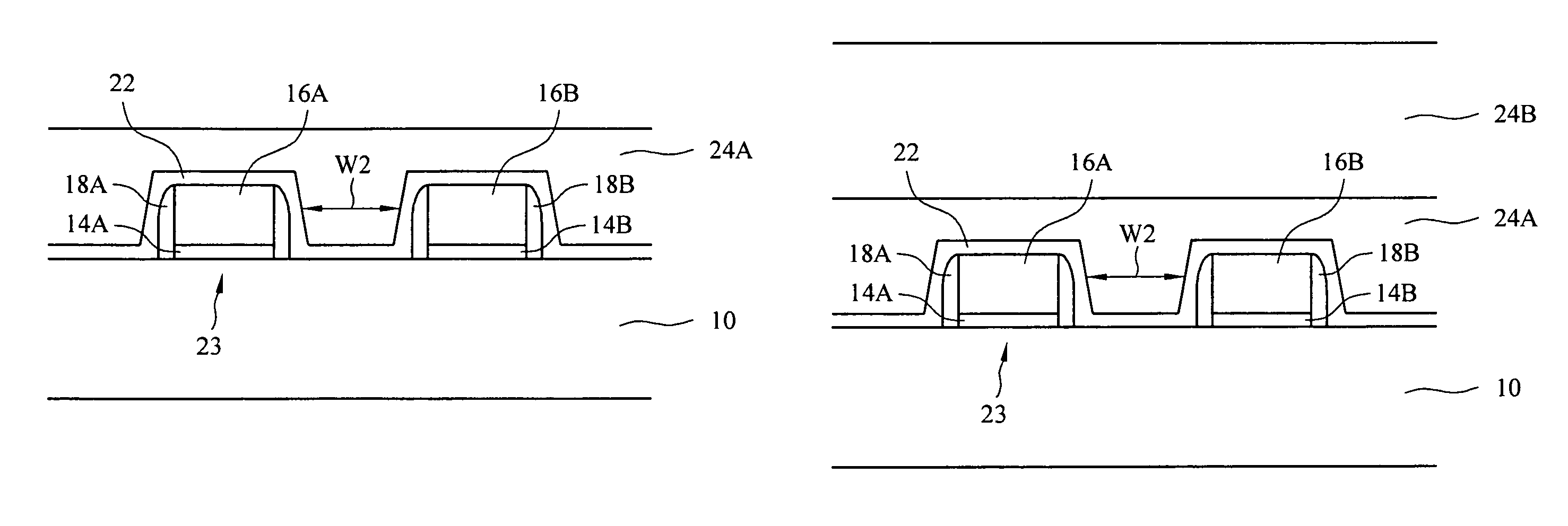
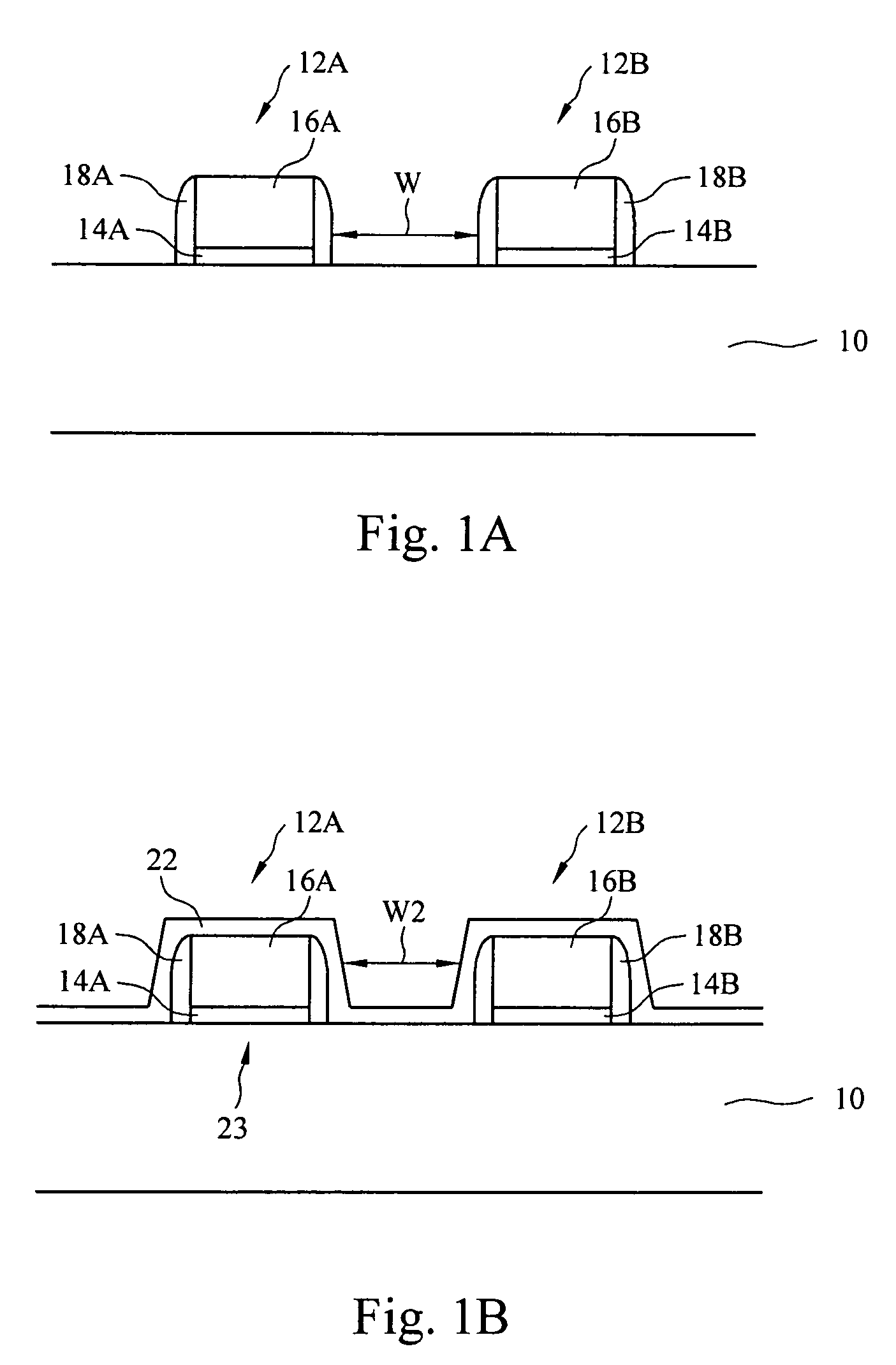
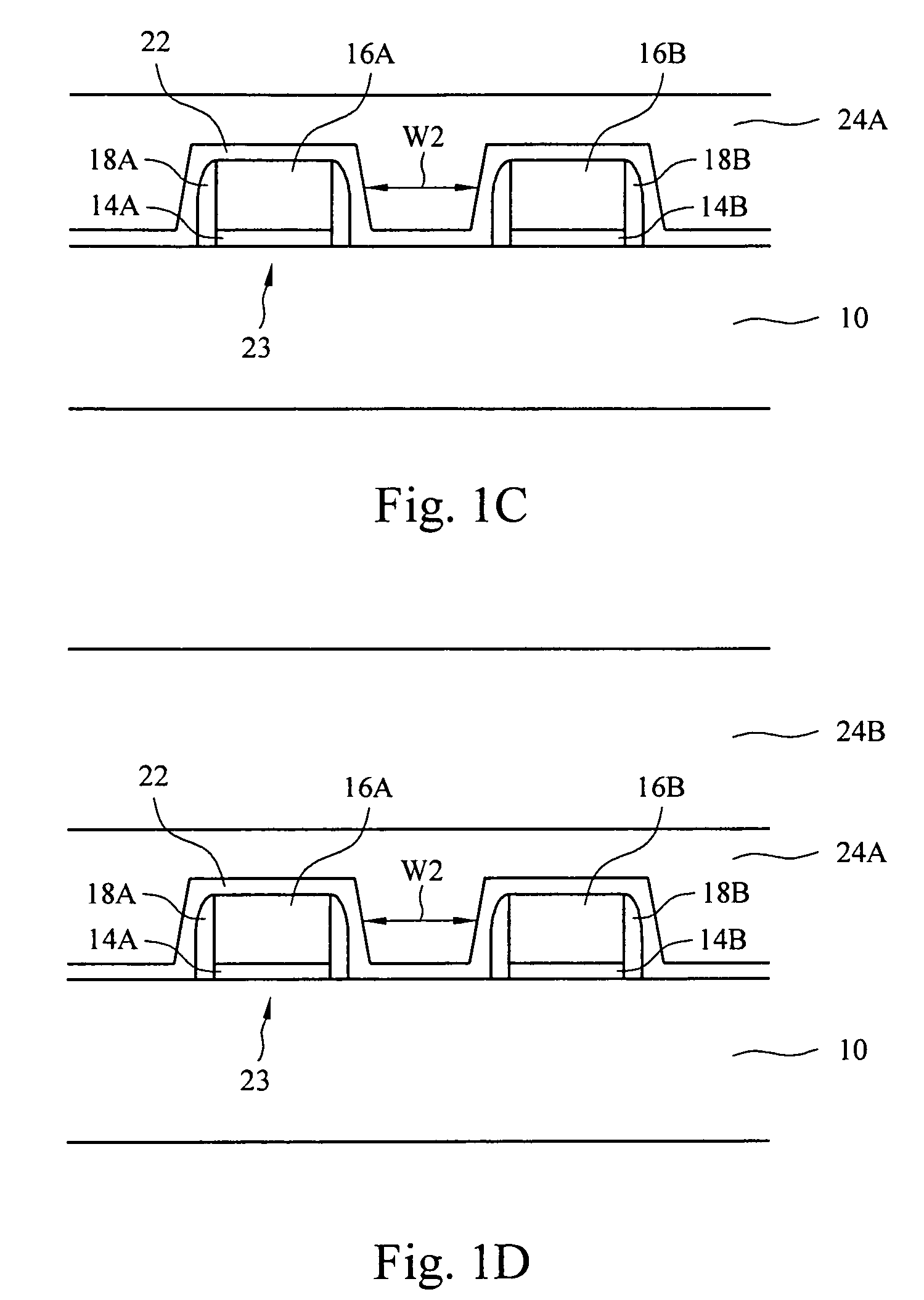
[0015]According to the present invention an HDP-CVD processing method is presented to improve a gap filling ability in a PMD layer deposition process, for example, avoid or reduce the formation of voids, while reducing plasma damage to CMOS devices and reducing a deposition temperature of the process wafer. It will be appreciated that a single or multi-step HDP-CVD process may be carried out optionally including cooling steps between deposition processes.

[0016]Referring to FIG. 1A, in an exemplary semiconductor manufacturing process for producing a pre-metal dielectric (PMD) layer, a semiconductor substrate 10 is provided including CMOS devices e.g., 12A and 12B, formed on the semiconductor substrate by conventional processes. For example, the semiconductor substrate 10 may include a variety of semiconductor substrates e.g., silicon, silicon on insulator (SOI), stacked SOI (SSOI), stacked SiGe on insulator (S-SiGeOI), SiGeOI, and GeOI, and combinations thereof. It will be appreciate...


PUM

PropertyMeasurementUnit
temperaturesaaaaaaaaaa
thicknessaaaaaaaaaa

Abstract

A method of forming an HDP-CVD pre-metal dielectric (PMD) layer to reduce plasma damage and / or preferential sputtering at a reduced a thermal budget including providing a semiconductor substrate comprising at least two overlying semiconductor structures separated by a gap; forming a PMD layer according to an HDP-CVD process over the at least two overlying semiconductor structures without applying a chucking bias Voltage to hold the semiconductor substrate.

Description

FIELD OF THE INVENTION[0001]This invention generally relates to HDP-CVD deposition processes and more particularly to a method for forming pre-metal dielectric (PMD) layers to improve a gap-filling ability and reduce plasma damage to advanced CMOS devices.BACKGROUND OF THE INVENTION[0002]As devices become smaller and integration density increases, high density plasma chemical vapor deposition (HDP-CVD) processes have become a key process due to superior gap-filling capability. In particular, high density plasma (HDP-CVD) processes, using plasma generating power sources such as electron cyclotron resonance (ECR) and inductively coupled plasma (ICP) processes produce high-quality silicon dioxide and silicon nitride layers. Generally, HDP-CVD provides a high density of plasma ions resulting in higher quality films at lower deposition temperatures compared to thermal process. HDP-CVD is particularly ideal for forming PMD oxide layers because of its superior gap filling capability. In an...

Claims


Application Information

Patent Timeline
Patent Type & Authority Patents(United States)
IPC IPC(8): H01L21/8238
CPCC23C16/509H01L21/02129H01L21/02164H01L21/02274H01L21/31612H01L21/76801H01L21/76837H01L29/7843H01L21/823871H01L29/78
Inventor CHEN, YAO-HSIANG
Owner TAIWAN SEMICON MFG CO LTD
Why Eureka
Try Eureka