Method for manufacturing self-aligned silicide barrier layer

A technology of self-aligned silicide and manufacturing method, which is applied in semiconductor/solid-state device manufacturing, electrical components, circuits, etc., and can solve problems that affect device performance and yield, design index threshold voltage shift, and cannot be completely removed. Achieve the effect of taking into account the etching rate and etching uniformity, improving device performance and product yield, and avoiding design index deviation

Active Publication Date: 2016-10-12
SHANGHAI HUAHONG GRACE SEMICON MFG CORP
View PDF5 Cites 3 Cited by
  • Summary
  • Abstract
  • Description
  • Claims
  • Application Information

AI Technical Summary

Problems solved by technology

During the etching process of the salicide barrier layer in the reaction chamber, if a higher etching power is used, such as greater than 300W, the etching rate of the salicide barrier layer is faster, but this will make the reaction The temperature of the cavity wall and the focus ring 12 (top ring) at the top of the wafer 20 is higher than that of the wafer 20, and the polymer (polymer) produced by etching will diffuse to the edge of the wafer 20, resulting in the middle area and edge of the wafer 20 There is

Method used


Image

  • Method for manufacturing self-aligned silicide barrier layer
  • Method for manufacturing self-aligned silicide barrier layer
  • Method for manufacturing self-aligned silicide barrier layer

Examples


Embodiment Construction

[0026] In order to make the purpose and features of the present invention more obvious and understandable, the specific implementation of the present invention will be further described below in conjunction with the accompanying drawings. However, the present invention can be implemented in different forms and should not be limited to the described embodiments.

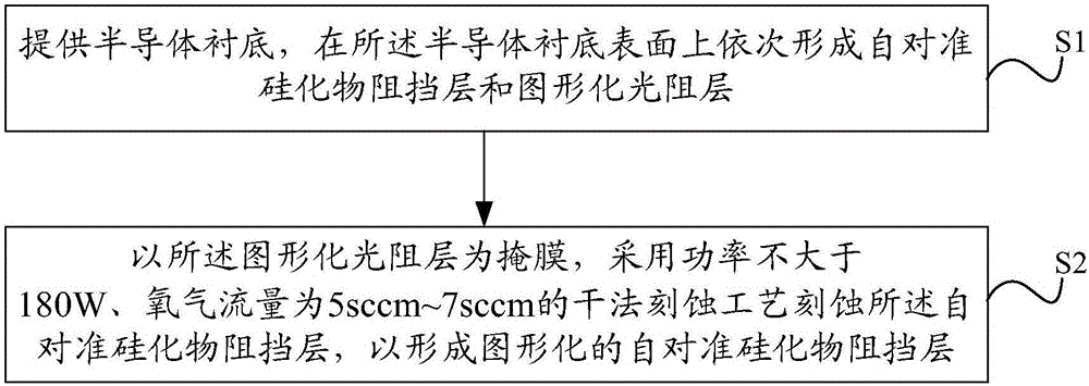
[0027] Please refer to figure 2 , the present invention provides a method for manufacturing a salicide barrier layer, comprising the following steps:

[0028] S1, providing a semiconductor substrate, sequentially forming a salicide barrier layer and a patterned photoresist layer on the surface of the semiconductor substrate;

[0029] S2, using the patterned photoresist layer as a mask, using a dry etching process with a power not greater than 180W and an oxygen flow rate of 5 sccm to 7 sccm to etch the salicide barrier layer to form a patterned self-aligned silicide barrier layer. alignment silicide barrier layer. ...


PUM


Abstract

The invention provides a method for manufacturing a self-aligned silicide barrier layer, which is characterized in that dry etching is carried out on the self-aligned silicide barrier layer by adopting the etching power being not greater than 180W and the oxygen flow rate of 5sccm-7sccm, plasma damages in the etching process can be reduced, diffusion of a polymer generated by etching towards the edge of a semiconductor substrate is reduced, and an effect of giving consideration to the etching rate and the etching uniformity is achieved, thereby acquiring a uniform graphical self-aligned silicide barrier layer with excellent performance, avoiding offset of device performance design indicators, and improving the product yield.

Description

technical field [0001] The invention relates to the field of semiconductor manufacturing, in particular to a method for manufacturing a self-aligned silicide barrier layer. Background technique [0002] In the semiconductor device manufacturing process, after forming the semiconductor device layer, it is necessary to form a metal silicide in a specific region to reduce the contact resistance. During this process, a self-aligned silicide block layer (Self-aligned silicide block layer, SAB) is generally required to protect the region on the semiconductor device layer where metal silicide does not need to be formed. The self-aligned silicide schemes widely used in the industry include a silicon oxide SAB layer and a silicon oxide / silicon nitride combined SAB layer. [0003] According to the manufacturing process of semiconductor devices, after the salicide barrier layer is formed, it is subjected to dry plasma etching so as to achieve a preset pattern and thickness. figure 1 ...

Claims


Application Information

Patent Timeline
IPC IPC(8): H01L21/311
CPCH01L21/31116H01L21/31144
Inventor 陈宏
Owner SHANGHAI HUAHONG GRACE SEMICON MFG CORP
Why Eureka
Try Eureka