Devices and methods for measuring nanometer level binding reactions

Inactive Publication Date: 2008-01-03
THE TRUSTEES OF COLUMBIA UNIV IN THE CITY OF NEW YORK
View PDF13 Cites 10 Cited by
  • Summary
  • Abstract
  • Description
  • Claims
  • Application Information

AI Technical Summary

Problems solved by technology

However, in the cell those proteins form into larger complexes or modules wherein the spacing of components on a nanometer scale is critical.

Method used


Image

  • Devices and methods for measuring nanometer level binding reactions
  • Devices and methods for measuring nanometer level binding reactions
  • Devices and methods for measuring nanometer level binding reactions

Examples


example 1

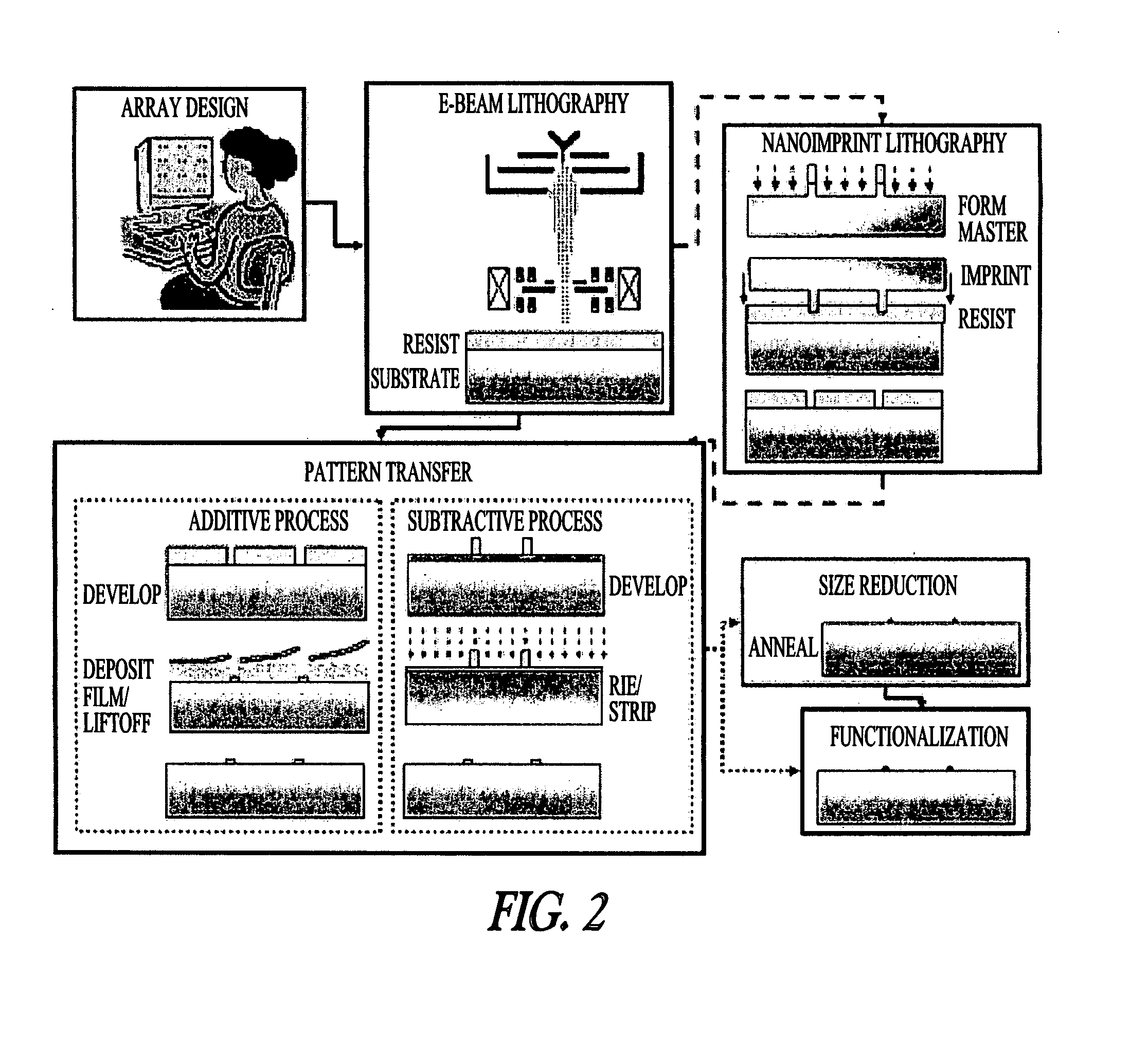
[0111] As shown in FIG. 2, a CAD software, such as CADENCE from SYNOPSIS or DESIGNCAD from IMSI, is utilized to form a pattern that can be utilized to form an array of posts. First, a thin layer of PMMA is deposited on a silicon wafer using spin casting. The pattern formed using the CAD software is transferred onto the PMMA layer utilizing electron beam lithography, such as a scanning electron microscope (FEI XL 30 SIRION) equipped with a NABITY NPGS pattern generator or a LEICA VB6-HR. After the pattern is transferred, the PMMA layer has regions of holes of approximately 5 to 20 nm. A thin layer of titanium (ranging from about 0.5 to 30 nms) is deposited on the surface of the wafer. Lift-off of the PMMA layer provides posts of titanium standing on the surface of the silicon wafer. Size reduction of the titanium posts is carried out under a non-oxidizing environment at about 400° C. for about 1 hour in argon or nitrogen gas. The titanium posts are oxidized to form posts of titanium ...

example 2

[0112] As shown in FIG. 2, a CAD software, such as CADENCE from SYNOPSIS or DESIGNCAD from IMSI, is utilized to form a pattern that can be utilized to form an array of pits. A thin layer of nickel is deposited on the silicon wafer surface followed by a thin layer of gold-palladium alloy (ranging from about 0.5 to 30 nms). The gold-palladium alloy is utilized because the grains of the gold-palladium alloy are significantly smaller than the gold and provide a smoother surface. A layer of PMMA (approximately 20 to 60 nm thick) is deposited on top of the gold-palladium alloy layer using spin casting. The pattern obtained using the CAD software is transferred onto the PMMA layer utilizing electron beam lithography, such as a scanning electron microscope (FEI XL 30 SIRION) equipped with a NABITY NPGS pattern generator or a LEICA VB6-HR. After pattern transfer, the PMMA layer has regions of holes of approximately 5 to 20 nm. Reactive ion etching or ion milling is carried out to form pits o...

example 3

[0113] As shown in FIG. 2, a CAD, such as CADENCE from SYNOPSIS or DESIGNCAD from IMSI, is utilized to form a pattern that can be utilized to form an array of pits. To carry out nanoimprint lithography, a master template is formed as follows. On a silicon wafer, PMMA layer is deposited and the pattern obtained from the CAD software is transferred onto the PMMA layer using electron beam lithography. Then, reactive ion etching or ion milling is carried to form posts of silicon. On a different silicon wafer, a layer of titanium is deposited and oxidized to form a layer of titanium dioxide. On top of the titanium dioxide layer, a layer of polystyrene is deposited using spin casting, where the thickness of the polystyrene layer is smaller or same as the height of the silicon posts described above. The silicon wafer having the polystyrene layer is heated above the glass transition temperature of the polystyrene (e.g., 180° C.) and the wafer having silicon posts is pressed onto the polysty...


PUM

PropertyMeasurementUnit
diameteraaaaaaaaaa
diameteraaaaaaaaaa
diameteraaaaaaaaaa

Abstract

Systems and methods for measuring nanometer level binding reactions are described herein. In some embodiments, the disclosed subject matter is directed to a device comprising (a) a substrate having a surface and (b) an ordered array of posts, pits, or patches over the surface, wherein the posts, pits, or patches are capable of binding a protein or small molecule ligand, and wherein the pitch between adjacent posts, pits, or patches is less than about 100 nm. In some other embodiments, the disclosed subject matter is also directed to methods for identifying the presence of an analyte in a fluid and to methods for measuring relative binding specificity or affinity between an analyte in a fluid and the posts, pits, or patches, using the device of the disclosed subject matter.

Description

[0001] This application claims the benefit of the filing date of International Application Serial No. PCT / US2004 / 034987, filed Oct. 15, 2004, and U.S. patent application Ser. No. 11 / 404,716, filed Apr. 13, 2006, both of which claim the benefit of provisional application U.S. Ser. No. 60 / 511,799, filed Oct. 15, 2003, which are hereby incorporated by reference into the subject application in their entireties. This application also claims the benefit of the filing date of provisional application U.S. Ser. No. 60 / 837,701, filed Aug. 15, 2006, which is hereby incorporated by reference into the subject application in its entirety.[0002] All patents, patent applications and publications cited herein are hereby incorporated by reference in their entirety. The disclosures of these publications in their entireties are hereby incorporated by reference into this application in order to more fully describe the state of the art as known to those skilled therein as of the date of the disclosed sub...

Claims


Application Information

Patent Timeline
Patent Type & Authority Applications(United States)
IPC IPC(8): G01N33/53C12M1/00C12M1/34C12M3/00G01NG01N33/543
CPCB82Y15/00B82Y30/00G01N33/6803G01N33/54373G01N33/54366
Inventor SHEETZ, MICHAEL P.WIND, SAMUEL J.
Owner THE TRUSTEES OF COLUMBIA UNIV IN THE CITY OF NEW YORK
Why Eureka
Try Eureka