
Integrated circuit with spare cells

a technology of integrated circuits and spare cells, applied in the field of integrated circuits, can solve problems such as many restrictions to correct such errors, devices cannot be added into integrated circuits after the complete manufacturing process, and bugs or faults in integrated circuits

Inactive Publication Date: 2008-02-07
VIA TECH INC
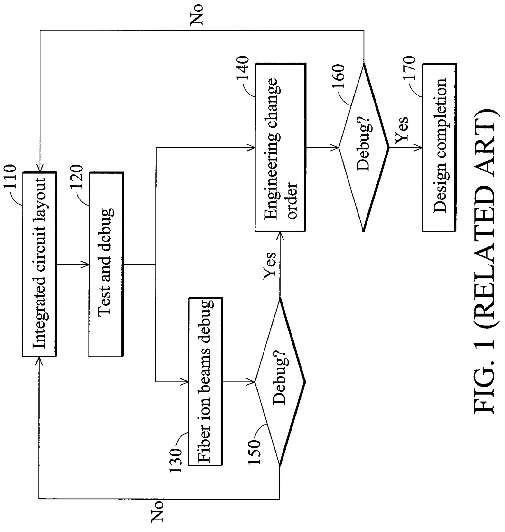
View PDF4 Cites 17 Cited by
  • Summary
  • Abstract
  • Description
  • Claims
  • Application Information

AI Technical Summary

Benefits of technology

The present invention provides an integrated circuit with spare cells that can be used to replace defective cells. The circuit includes a substrate and a plurality of metal patterns and vias that connect the input and output terminals of the spare cells to a power or ground voltage. The metal layers are arranged in a stacked structure, which helps to conserve routing resources. The technical effect of this invention is to provide a reliable and flexible way to manufacture integrated circuits with spare cells.

Problems solved by technology

There may be a bug or a fault existing in the integrated circuits because of the mistake in designing.
However, there are many restrictions to correct such a mistake.
For example, the devices cannot be added into integrated circuits after the complete manufacturing processes.
However, there are many restrictions to perform the fiber ion beam (FIB) revision.
When engineering change orders are performed to replace the spare cell with the standard cell, a plurality of masks must be conventionally revised, with design cost increased accordingly

Method used


Image

  • Integrated circuit with spare cells
  • Integrated circuit with spare cells
  • Integrated circuit with spare cells

Examples


Embodiment Construction

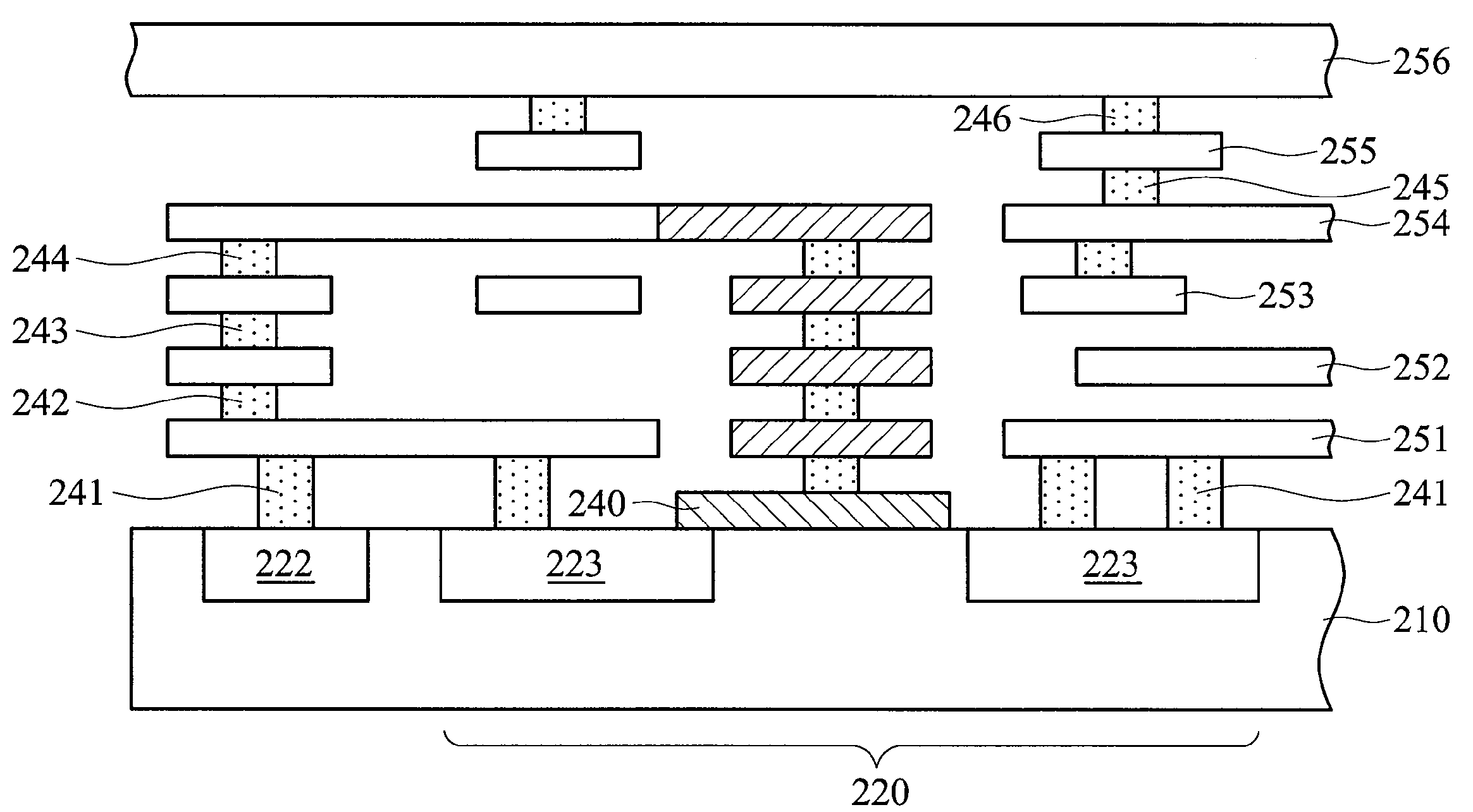
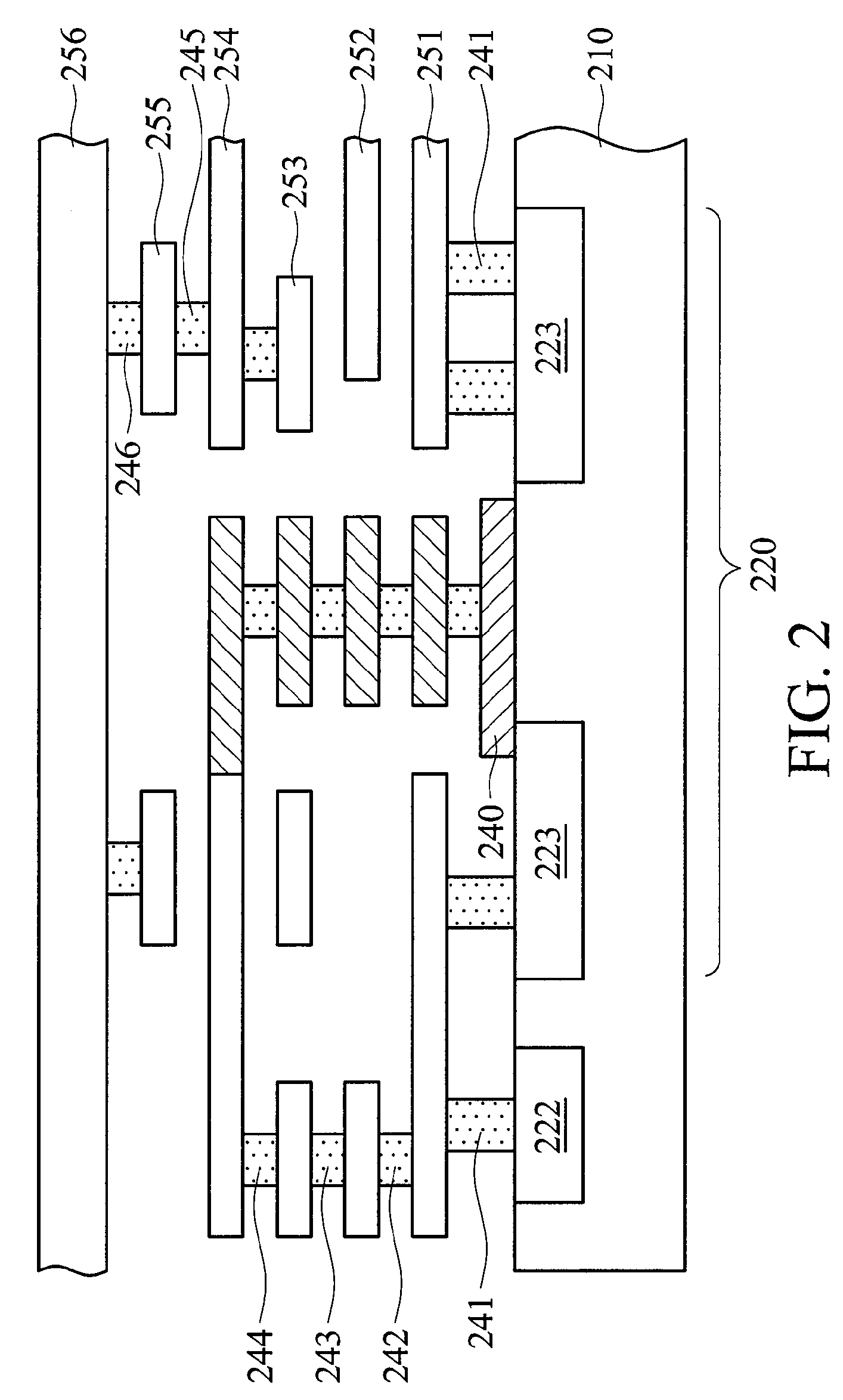
[0027]FIG. 2 shows an embodiment of an integrated circuit 200 with spare cells, comprising a p-type silicide structure and six stacked metal layers (1P6M integrated circuit). A standard cell, a spare cell 220, and a ploysilicon layer are formed on the substrate 210.

[0028]The spare cell 220 comprises a negative-channel metal oxide semiconductor (NMOS) transistor. The substrate 210 can be a p-type silicide structure and comprise a p+ doping region 222 and two n+ doping regions 223, wherein the two ends of the polysilicon layer 240 are located in the two n+ doping regions 223 respectively.

[0029]The polysilicon layer 240 serves as the gate electrode of the negative-channel metal oxide semiconductor (NMOS) transistor. One of the n+ doping regions 223 service as the source electrode of the NMOS transistor and the other n+ doping region 223 is the drain electrode of the NMOS transistor. In addition, the p+ doping region 222 is the bulk electrode of the NMOS transistor. After routing and co...


PUM


Abstract

An integrated circuit with spare cells. The integrated circuit comprises a substrate, spare cells formed on the substrate, and a plurality of metal layers and metal vias stacked over an input or output. A metal layer outermost from the substrate, among the plurality of metal layers, electrically connects to a power or ground voltage.

Description

BACKGROUND OF THE INVENTION[0001]1. Field of the Invention[0002]The invention relates to an integrated circuit, and, more particularly, to an integrated circuit with spare cells.[0003]2. Description of the Related Art[0004]Development of integrated circuits normally comprises continuous tests, debugging and revision (including addition / removal of devices and cutting / connecting conductive wires) for samples designed thereby.[0005]There may be a bug or a fault existing in the integrated circuits because of the mistake in designing. However, there are many restrictions to correct such a mistake. For example, the devices cannot be added into integrated circuits after the complete manufacturing processes. Thus, spare cells or gates are pre-provided in the integrated circuit layout during the circuits designing to correct the logic mistake in designing. The spare cells have preset electrical or logic function, which is similar to the standard cells or standard logic gates expect that the ...

Claims


Application Information

Patent Timeline
Patent Type & Authority Applications(United States)
IPC IPC(8): H01L27/10
CPCG11C5/063H01L27/11807H01L27/0207
Inventor FAN, DE-AN
Owner VIA TECH INC
Learn More