Laminating System, Ic Sheet, Scroll of Ic Sheet, and Method for Manufacturing Ic Chip

a technology of ic chip and ic sheet, which is applied in the direction of chemistry apparatus and processes, instruments, printing, etc., can solve the problems of deteriorating manufacturing efficiency, difficult sealing of thin film integrated circuits, and failure of peeling so as to prevent deterioration of manufacturing efficiency, prevent damage and destruction of thin film integrated circuits, and improve manufacturing yields

Inactive Publication Date: 2008-02-21
SEMICON ENERGY LAB CO LTD
View PDF21 Cites 108 Cited by
  • Summary
  • Abstract
  • Description
  • Claims
  • Application Information

AI Technical Summary

Benefits of technology

[0010] In view of the foregoing, it is an object of the present invention to prevent deterioration of manufacturing efficiency when sealing thin film integrated circuits and to prevent damage and destruction of the thin ...

Problems solved by technology

When the separated thin film integrated circuits are respectively sealed by laminate treatment or the like, manufacturing efficiency is deteriorated.
Since the separated thin film integrated circuits are thin and lightweight, it is extremely difficult to seal them without damaging or breaking.
Hence, when peeling process for the thin film integrated circuits is also carried out with a film having strong adhesion force, peeling of the thin film inte...

Method used


Image

  • Laminating System, Ic Sheet, Scroll of Ic Sheet, and Method for Manufacturing Ic Chip
  • Laminating System, Ic Sheet, Scroll of Ic Sheet, and Method for Manufacturing Ic Chip
  • Laminating System, Ic Sheet, Scroll of Ic Sheet, and Method for Manufacturing Ic Chip

Examples


embodiment 1

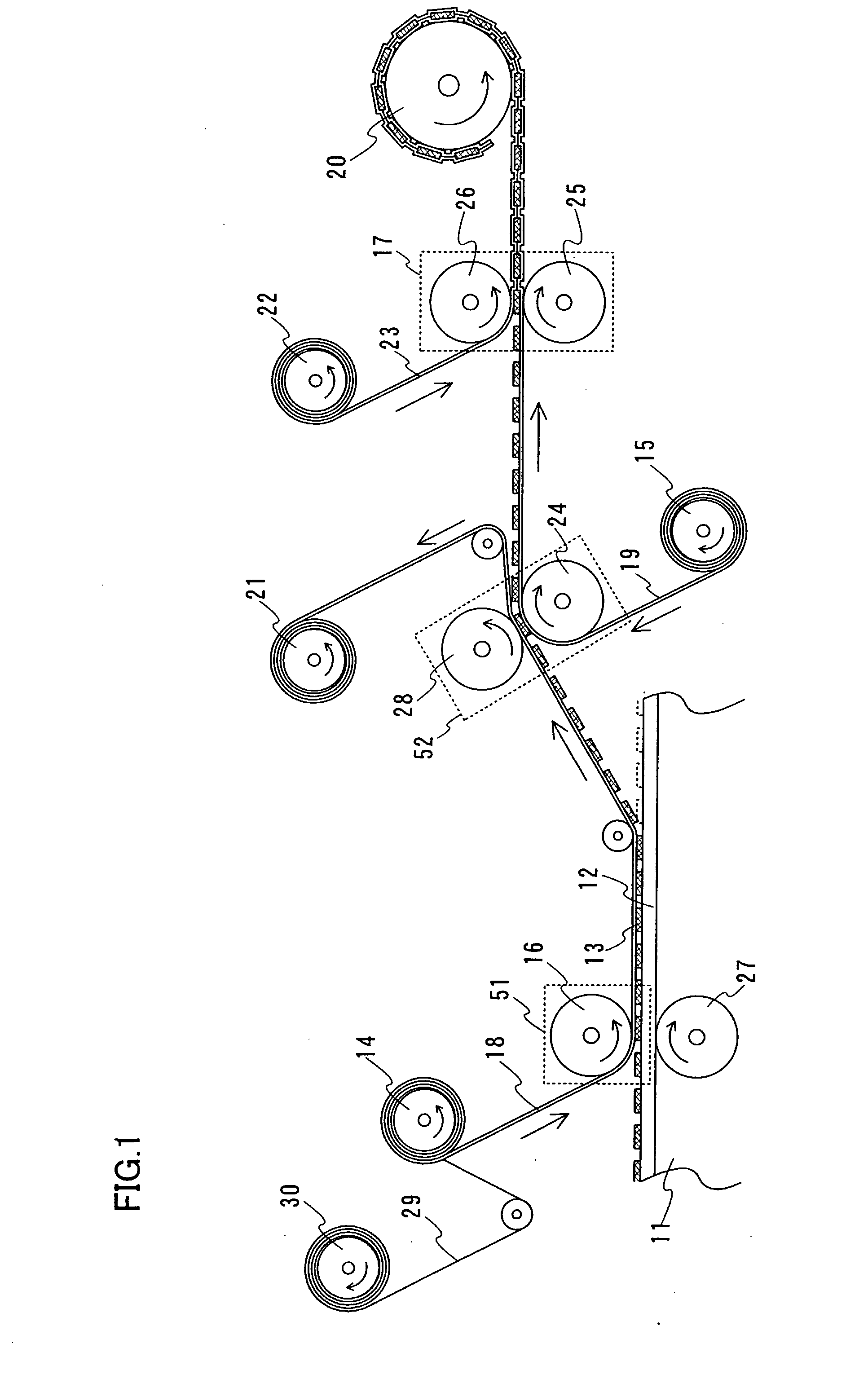
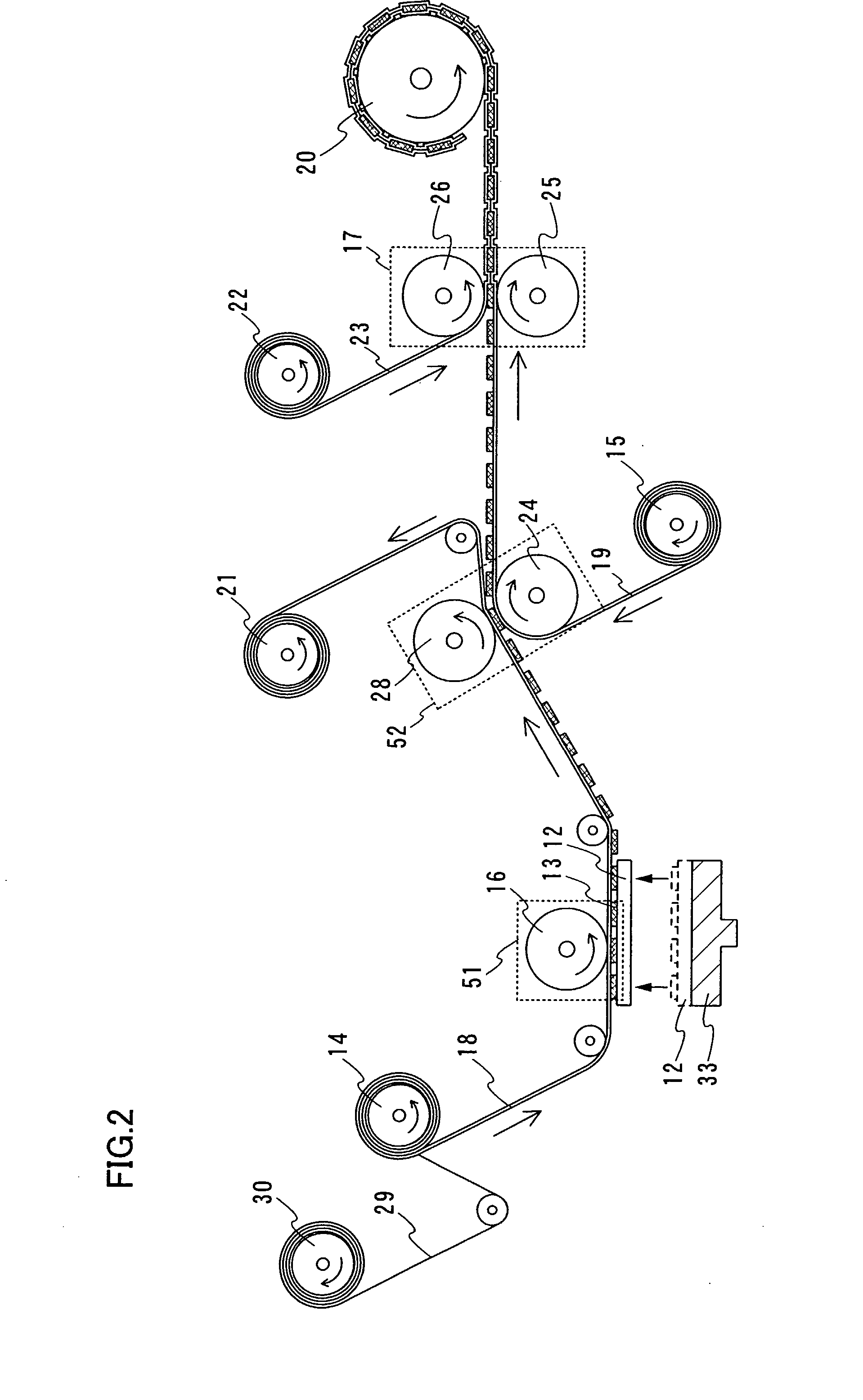
[0045] In this embodiment, a main form of a laminating system for continuously performing processes of peeling thin film integrated circuits from a substrate and sealing the peeled thin film integrated circuits will be hereinafter explained.

[0046] The laminating system according to this embodiment has a transporting means 11 for transporting a substrate 12 provided with a plurality of thin film integrated circuits 13, a first supply roller 14 winded with a first sheet member 18, a first peeling means 51 provided with a roller 16 for bonding the thin film integrated circuits 13 to the first sheet member 18 to peel the thin film integrated circuits 13 from the substrate 12, a second supply roller 15 winded with a second sheet member 19, a second peeling means 52 provided with rollers 24, 28 for bonding the thin film integrated circuits 13 to a second sheet member 19 to peel the thin film integrated circuits 13 from the first sheet member 18, a receiving roller 21 for collecting the f...

embodiment 2

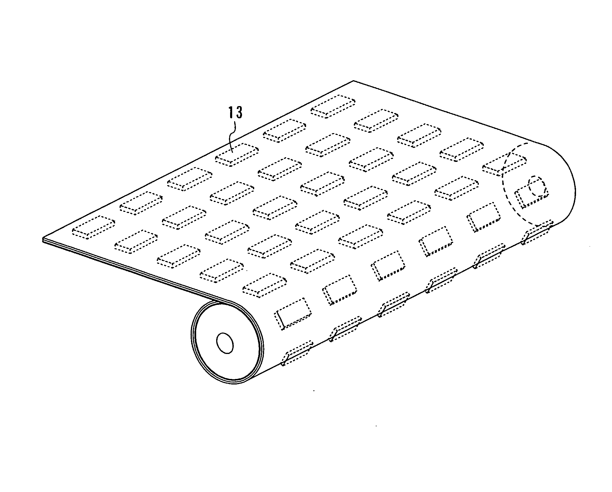
[0082] In this embodiment, the structure of an IC sheet (also referred to as an IC film, a sheet member, or a film member) is explained hereinafter.

[0083] As illustrated in FIG. 5, the IC sheet is a sheet formed by interposing to seal each of thin film integrated circuits 13 between two sheet members 19 and 23. The IC sheet is obtained by interposing to seal a plurality of thin film integrated circuits between the second sheet member 19 and the third sheet member 23 as shown in Embodiment 1.

[0084] Each of the thin film integrated circuits 13 has a plurality of elements and a conductive layer serving as an antenna. Moreover, each of the thin film integrated circuits 13 can be regularly arranged to be a sheet by peeling effectively the thin film integrated circuits provided over the substrate (FIG. 5A). Further, one IC sheet may be rolling up in a roller or may be folded back on itself (FIG. 5B).

[0085] As noted above, it is easy to ship the sheet-like IC sheet including a plurality...

embodiment 3

[0087] In this embodiment, the structure of a scroll of an IC sheet is explained hereinafter.

[0088] As illustrated in FIG. 6, the scroll of the IC sheet is formed by reeling a sheet member. Specifically, the scroll of the IC sheet is formed by reeling a plurality of thin film integrated circuits 13 which is interposed to be sealed between two sheet members 19 and 23 to be a roll. As described in Embodiment 1, the scroll of the IC sheet is obtained by reeling by a roller to collect the sheet-like plurality of thin film integrated circuits 13 sealed with a second sheet member 19 and a third sheet member 23. Each of the thin film integrated circuits 13 has a plurality of elements and a conductive layer serving as an antenna. Moreover, each of the thin film integrated circuits 13 is regularly arranged.

[0089] As noted above, it is easy to ship the scroll of the IC sheet formed by reeling the thin film integrated circuits 13 sealed with a pair of sheet members. Particularly, the scroll ...


PUM

PropertyMeasurementUnit
Pressureaaaaaaaaaa
Electrical conductoraaaaaaaaaa
Adhesivityaaaaaaaaaa

Abstract

Thin film integrated circuits are peeled from a substrate and the peeled thin film integrated circuits are sealed, efficiently in order to improve manufacturing yields. The present invention provides laminating system comprising transporting means for transporting a substrate provided with a plurality of thin film integrated circuits; first peeling means for bonding first surfaces of the thin film integrated circuits to a first sheet member to peel the thin film integrated circuits from the substrate; second peeling means for bonding second surfaces of the thin film integrated circuits to a second sheet member to peel the thin film integrated circuits from the first sheet member; and sealing means for interposing the thin film integrated circuits between the second sheet member and a third sheet member to seal the thin film integrated circuit with the second sheet member and the third sheet member.

Description

TECHNICAL FIELD [0001] The present invention relates to a laminating system for peeling and sealing thin film integrated circuits provided over a substrate, an IC sheet including a plurality of sealed thin film integrated circuits, a scroll of an IC sheet including a plurality of sealed thin film integrated circuits, and a method for manufacturing an IC chip which seals thin film integrated circuits. BACKGROUND ART [0002] In recent years, the necessity of an IC chip mounted card or an IC chip mounted tag which can transmit data out of touch has been grown in a field which needs automatic recognition such as securities and commodity management. The IC chip mounted card reads and writes data to / from an external device via a loop antenna in the card. The IC chip mounted card has larger memory capacity and higher security than those of a magnetic card that records data by a magnetic encoding method. Hence, it has been proposed that a form of the IC mounted card capable of being applied ...

Claims


Application Information

Patent Timeline
IPC IPC(8): H01L27/10B29C65/00B32B37/00
CPCB32B37/0053H01L2924/01041B32B2425/00G06K19/077G06K19/07718H01L24/86H01L27/1214H01L27/1266H01L2224/7965H01L2924/01002H01L2924/01004H01L2924/01005H01L2924/01013H01L2924/01015H01L2924/01027H01L2924/01029H01L2924/01033H01L2924/01042H01L2924/01049H01L2924/01056H01L2924/0106H01L2924/01073H01L2924/01074H01L2924/01079H01L2924/01082H01L2924/04953H01L2924/09701H01L2924/14H01L2924/19041H01L2924/01006H01L2924/01024B32B37/226H01L2924/15787H01L2924/00B29C65/02B42D25/45G06K19/07
Inventor WATANABE, RYOSUKEKUSUMOTO, NAOTONAKAMURA, OSAMU
Owner SEMICON ENERGY LAB CO LTD
Why Eureka
Try Eureka