
Method of forming a material layer

a technology of material layer and layer layer, which is applied in the direction of coating, chemical vapor deposition coating, plasma technique, etc., can solve the problems of contamination particles during subsequent processes, unfavorable diffusion of metal layers into surrounding material layers, and reduced design rules for semiconductor devices

Inactive Publication Date: 2008-02-21
SAMSUNG ELECTRONICS CO LTD
View PDF6 Cites 83 Cited by
  • Summary
  • Abstract
  • Description
  • Claims
  • Application Information

AI Technical Summary

Benefits of technology

[0009]Example embodiments of the present invention provide a method that is capable of forming a material layer on a wafer without generating a powdery contamination layer on exposed inner surfaces of a process chamber.

Problems solved by technology

The undesired diffusion of a metal layer into surrounding material layers has become a significant problem as the design rules for semiconductor devices has been reduced.
This accumulation of nickel fluoride (NiF2) and / or aluminum fluoride (AlF3) may adversely affect process reproducibility and / or generate contamination particles during subsequently performed processes.
Furthermore, the aluminum fluoride (AlF3) and / or the nickel fluoride (NiF2) formed by the foregoing may inhibit the effective remove of titanium and / or the titanium nitride layers from the inner surfaces of the process chamber.

Method used


Image

  • Method of forming a material layer
  • Method of forming a material layer
  • Method of forming a material layer

Examples


Embodiment Construction

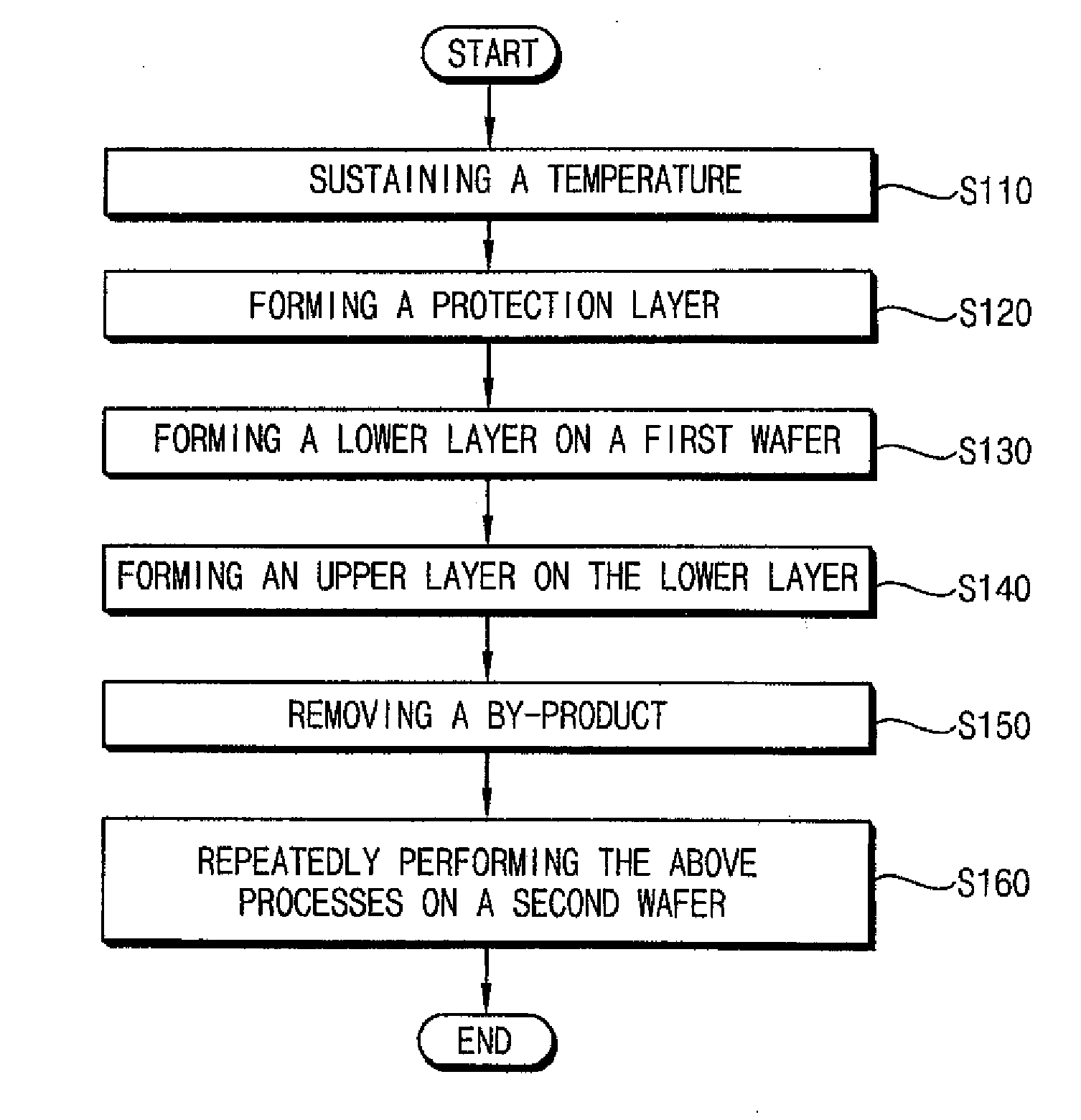
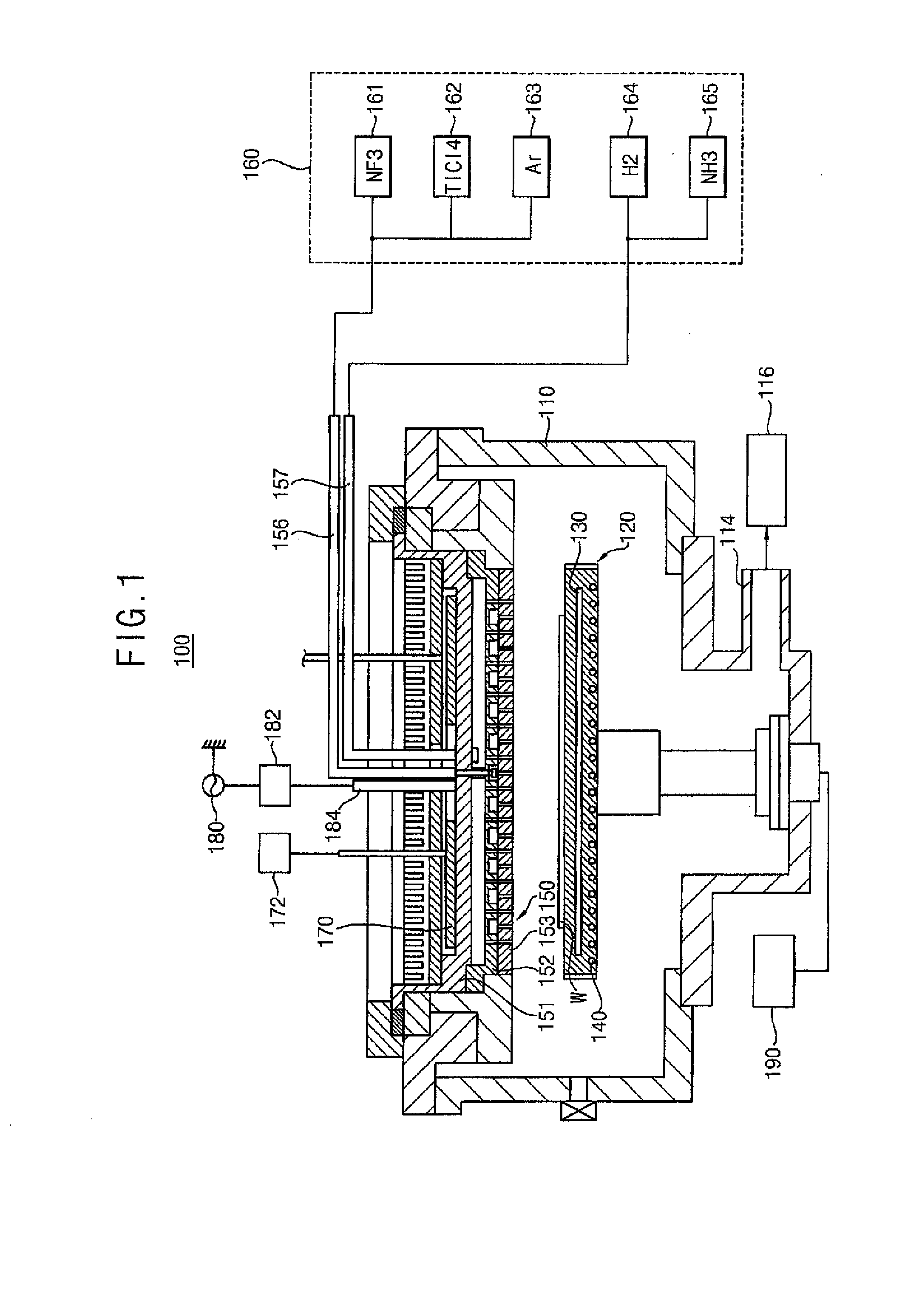
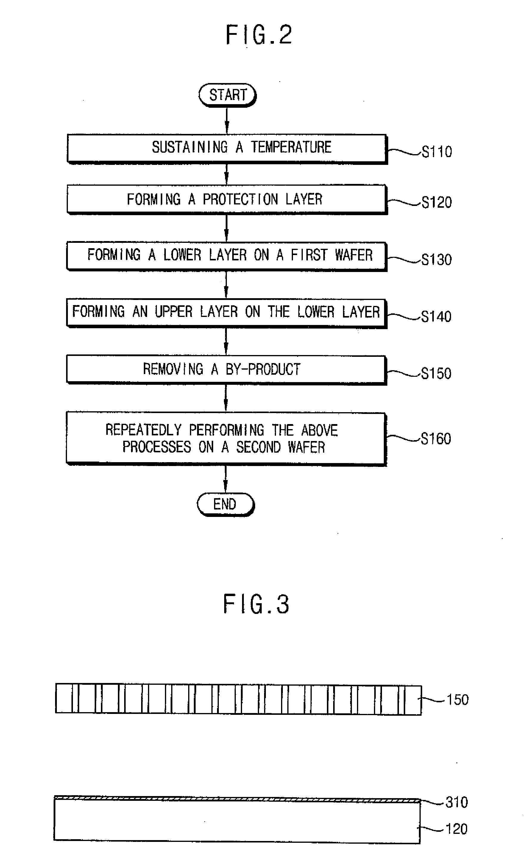
[0016]Embodiments of the invention will now be described with reference to the accompanying drawings. This invention may, however, be embodied in many different forms and should not be construed as being limited to only the embodiments set forth herein. In the drawings, the size and relative sizes of layers and regions may be exaggerated for clarity. Throughout the drawings and written description, like reference numbers refer to like or similar elements.

[0017]It will be understood that when an element or layer is referred to as being “on,”“connected to” or “coupled to” another element or layer, it can be directly on, connected or coupled to the other element or layer or intervening elements or layers may be present. In contrast, when an element is referred to as being “directly on,”“directly connected to” or “directly coupled to” another element or layer, there are no intervening elements or layers present. As used herein, the term “and / or” includes any and all combinations of one ...


PUM

PropertyMeasurementUnit
Temperatureaaaaaaaaaa

Abstract

A method of processing a wafer in a chamber including a wafer stage and a showerhead is disclosed. The method includes forming a first protection layer on the wafer stage, heating the wafer stage to a first temperature, heating the showerhead at a second temperature lower than the first temperature, forming a second protection layer on inner surfaces of the process chamber including at least the wafer stage and showerhead, loading a wafer onto the wafer stage, forming a material layer on the wafer, and then unloading the wafer from the wafer stage, and removing by-products generated on the inner surfaces of the process chamber during formation of the material layer while maintaining the first temperature of the wafer stage and the second temperature of the showerhead.

Description

CROSS-REFERENCE TO RELATED APPLICATION[0001]This application claims priority under 35 USC §119 to Korean Patent Application No. 2006-77748 filed Aug. 17, 2006, the subject matter of which is hereby incorporated by reference.BACKGROUND OF THE INVENTION[0002]1. Field of the Invention[0003]The present invention relates to a method of forming a material layer on a wafer disposed in a process chamber.[0004]2. Description of the Related Art[0005]The manufacture of contemporary semiconductor devices involves the application of numerous fabrication processes. Some of these fabrication processes form desired material layers on a subject wafer. The material layers are subsequently patterned and connected to form functional circuits including constituent circuit elements. Amongst the many different material layers formed on wafers are various metal layers. The undesired diffusion of a metal layer into surrounding material layers has become a significant problem as the design rules for semicond...

Claims


Application Information

Patent Timeline
IPC IPC(8): H05H1/24C23C16/00
CPCC23C16/08C23C16/34C23C16/4557C23C16/45565C23C16/4405H01L21/20
Inventor SEO, JUNG-HUNLEE, EUN-TAECKKIM, SOO-HWAN
Owner SAMSUNG ELECTRONICS CO LTD
Features
  • Generate Ideas
  • Intellectual Property
  • Life Sciences
  • Materials
  • Tech Scout
  • Unparalleled Data Quality
  • Higher Quality Content
  • 60% Fewer Hallucinations
Learn More