
Liquid crystal display device and electronic apparatus

a display device and liquid crystal technology, applied in non-linear optics, instruments, optics, etc., can solve the problems of low productivity compared with the rubbing process using the rubbing cloth, light leakage or decrease in the alignment regulating force, etc., to reduce the burn-in of the display

Active Publication Date: 2008-03-06
JAPAN DISPLAY WEST
View PDF11 Cites 4 Cited by
  • Summary
  • Abstract
  • Description
  • Claims
  • Application Information

AI Technical Summary

Benefits of technology

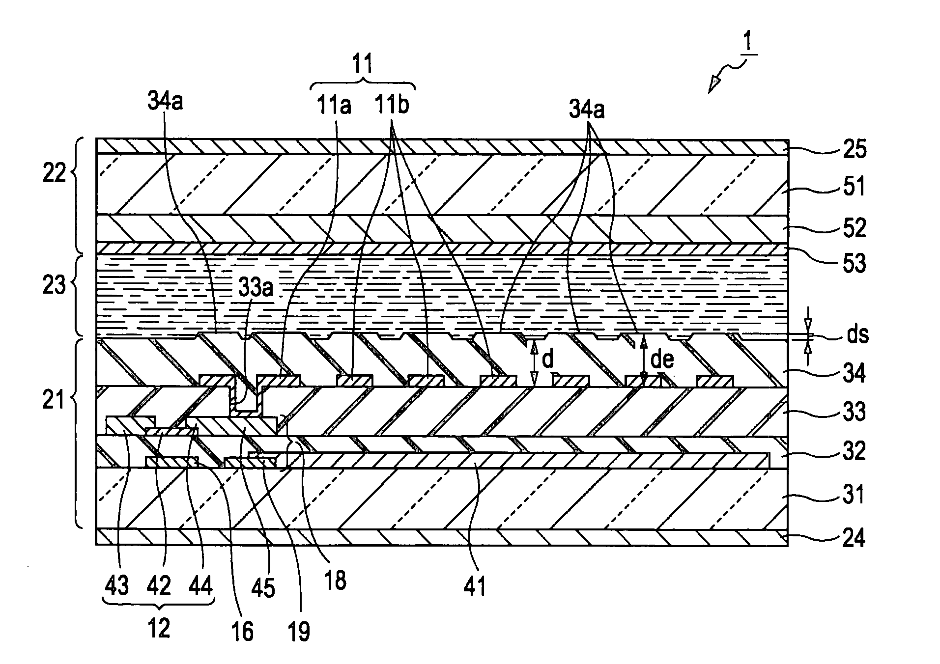
[0011]In the invention, since the thickness of the electrode contacting the alignment film is larger than that of the alignment film, the flatness of the alignment film is improved, a rubbing process is uniformly performed, and display burn-in due to an alignment regulation failure can be reduced.
[0031]In the invention, since the thickness of the electrode contacting the alignment film is larger than that of the alignment film, it is possible to reduce display burn-in and to perform good image display, as described above.

Problems solved by technology

Accordingly, a rubbing process is non-uniformly performed on the step difference portion and the other points and thus light leakage or decrease in alignment regulating force occurs.
However, even in this alignment process, the following problems occur.
That is, in the optical alignment process, the alignment regulating force of liquid crystal molecules due to the alignment film is small and it is difficult to uniformly perform the alignment process.
In addition, productivity is low compared with the rubbing process using the rubbing cloth.

Method used


Image

  • Liquid crystal display device and electronic apparatus
  • Liquid crystal display device and electronic apparatus
  • Liquid crystal display device and electronic apparatus

Examples


first embodiment

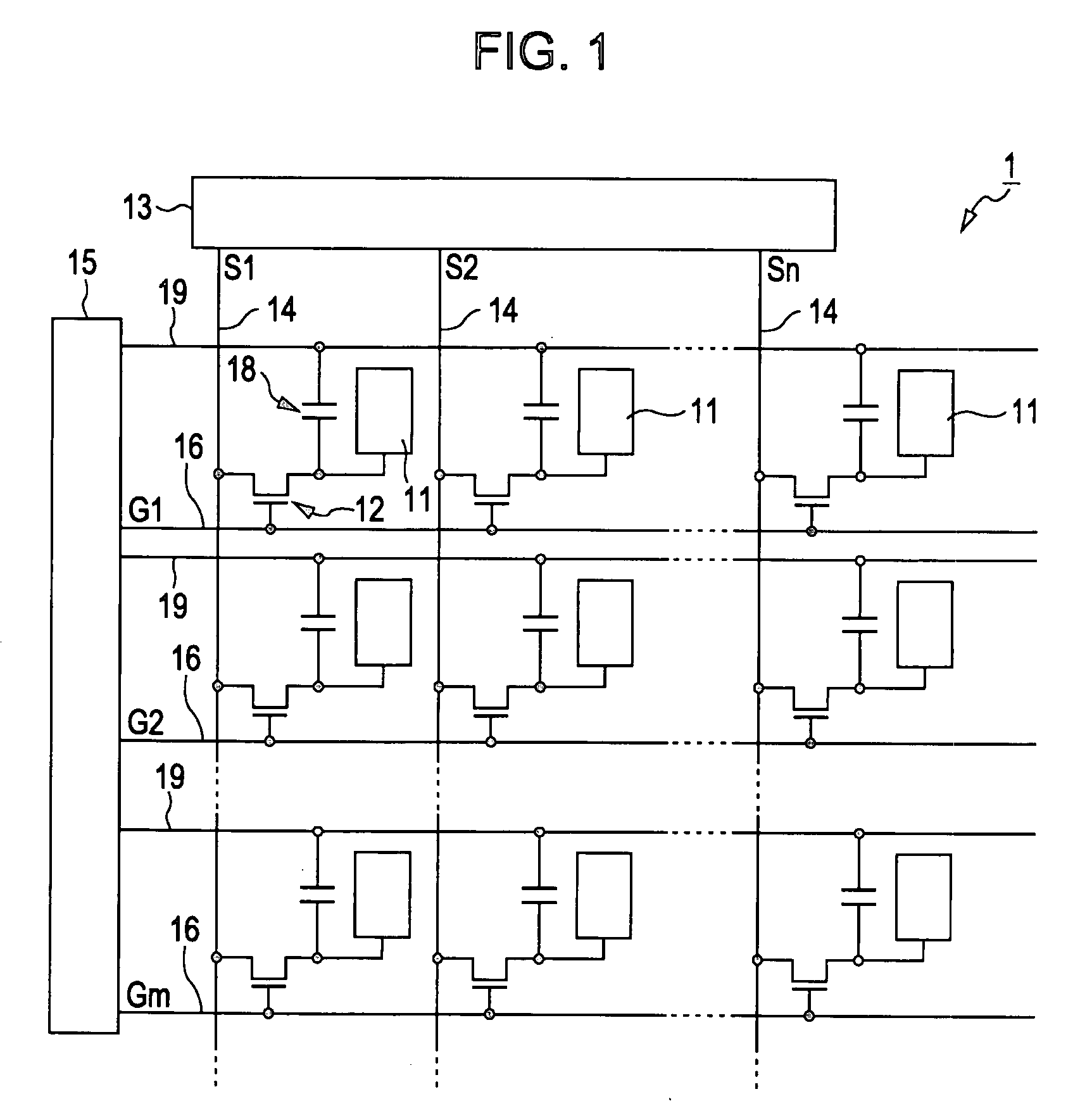
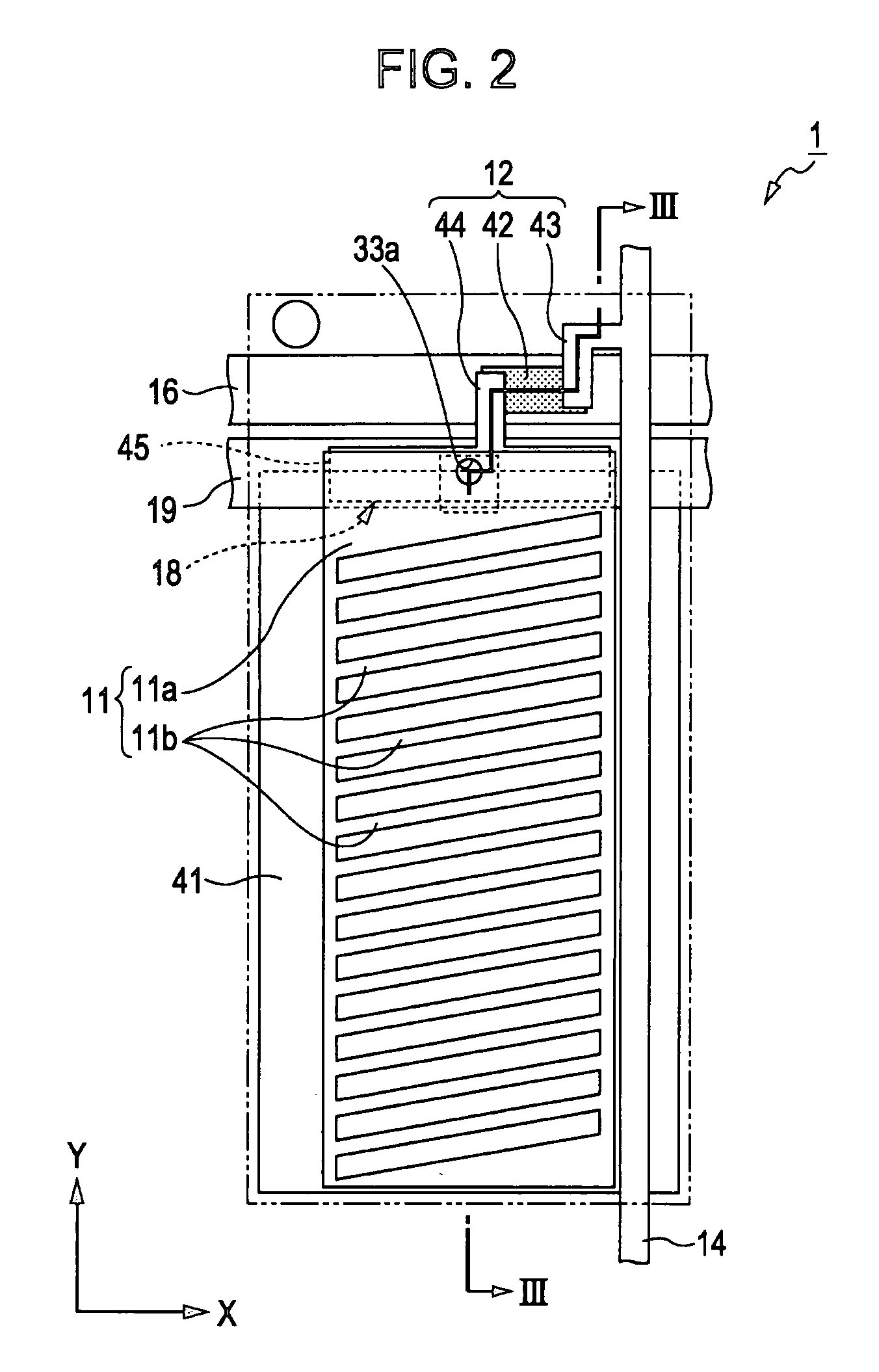
[0044]Hereinafter, a liquid crystal display device according to a first embodiment of the invention will be described with reference to the accompanying drawings. In each view used for following description, the scale of each layer or each element is differentiated from others such that each layer or each element has a size such that it can be easily identified in the view. FIG. 1 is an equivalent circuit diagram of the liquid crystal display device, FIG. 2 is a partial enlarged plan view showing a sub pixel region of the liquid crystal display device, FIG. 3 is a cross-sectional view taken along line III-III of FIG. 2, and FIG. 4 is a view showing an arrangement of an optical axis of FIG. 2.

Liquid Crystal Display Device

[0045]The liquid crystal display device 1 according to the present embodiment is a FFS liquid crystal display device in which three sub pixels for outputting color light of red (R), green (G) and blue (B) configure one pixel. Here, a display region which is a minimum...

second embodiment

[0089]Next, a liquid crystal display device according to a second embodiment of the invention will be described with reference to the accompanying drawings. Since the present embodiment is different from the first embodiment in the configuration of the pixel electrode, the second embodiment will be described concentrating on the configuration of the pixel electrode. The components described in the first embodiment are denoted by same reference numerals and thus the description thereof will be omitted. FIG. 7 is a partial enlarged plan view showing a sub pixel region of the liquid crystal display device according to the second embodiment of the invention.

[0090]In the liquid crystal display device 110 according to the present embodiment, as shown in FIG. 7, a pixel electrode 111 has substantially a comb shape in plan view. That is, the pixel electrode 111 includes a band-shaped connection portion 111a and a plurality (fifteen) of band-shaped electrodes 111b which are branched from the...

third embodiment

[0096]Next, a liquid crystal display device according to a third embodiment of the invention will be described with reference to the accompanying drawings. Since the present embodiment is different from the first embodiment in the configuration of the pixel electrode, the third embodiment will be described concentrating on the configuration of the pixel electrode. The components described in the first embodiment are denoted by same reference numerals and thus the description thereof will be omitted. FIG. 8 is a partial enlarged plan view showing a sub pixel region of the liquid crystal display device.

[0097]In the liquid crystal display device 120 according to the present embodiment, as shown in FIG. 8, a pixel electrode 121 includes a frame portion 11a having substantially a trapezoidal shape in plan view and a plurality of band-shaped electrodes 121a.

[0098]Curved portions 121b and 121c are formed in both ends of the band-shaped electrodes 121a connected to the frame portion 11a. T...


PUM

PropertyMeasurementUnit
thicknessaaaaaaaaaa
thicknessaaaaaaaaaa
thicknessaaaaaaaaaa

Abstract

Disclosed herein is a liquid crystal display device in which a plurality of electrodes is provided on one of a plurality of substrates with a liquid crystal layer interposed therebetween and liquid crystal molecules configuring the liquid crystal layer are driven by an electric field generated between the pair of electrodes, wherein the one substrate has an alignment film which contacts the liquid crystal layer to regulate an alignment direction of the liquid crystal molecules and is provided so as to cover at least one of the pair of electrodes, and wherein the thickness of the alignment film is larger than that of at least one of the electrodes contacting the alignment film.

Description

[0001]The entire disclosure of Japanese Patent Application Nos. 2006-239408, filed Sep. 4, 2006 and 2007-193405, filed Jul. 25, 2007 are expressly incorporated by reference herein.BACKGROUND[0002]1. Technical Field[0003]The present invention relates to a liquid crystal display device using a lateral electric field drive system and an electronic apparatus including the same.[0004]2. Related Art[0005]In order to realize a wide viewing angle of a liquid crystal display device, a system for generating an electric field in a liquid crystal layer toward a substrate direction and controlling alignment of liquid crystal molecules (hereinafter, referred to as a lateral electric field system) is known. Examples of the lateral electric field system include an in-plane switching (IPS) system and a fringe-field switching (FFS) system.[0006]In general, in a lateral electric field liquid crystal display device, a pair of electrodes for driving a liquid crystal layer is provided on one of a pair of...

Claims


Application Information

Patent Timeline
Patent Type & Authority Applications(United States)
IPC IPC(8): G02F1/1337
CPCG02F1/1337G02F1/1362G02F1/134363
Inventor KURASAWA, HAYATO
Owner JAPAN DISPLAY WEST
Learn More