Eureka AIR delivers breakthrough ideas for toughest innovation challenges, trusted by R&D personnel around the world.

Method and system for automated path delay test vector generation from functional tests

a technology of functional test and vector generation, applied in the field of integrated circuit design and fabrication, can solve the problems of large size and complexity of circuit design, inability to achieve pdt test vector generation successfully on a small portion of paths, and time-consuming functional test generation for an ate, so as to increase the pdt test coverage

Active Publication Date: 2008-04-17
ORACLE INT CORP
View PDF7 Cites 10 Cited by
  • Summary
  • Abstract
  • Description
  • Claims
  • Application Information

AI Technical Summary

Benefits of technology

[0007]The present invention addresses the above-described limitations of testing a design of an integrated circuit and, in turn, testing of a fabricated representation of the circuit design. An approach is disclosed to increase PDT test coverage for a given circuit design. As taught by the present invention, PDT test vectors are generated from functional simulation of a representation of the circuit design avoiding the reliance on test point and test node access to the paths forming the circuit design.
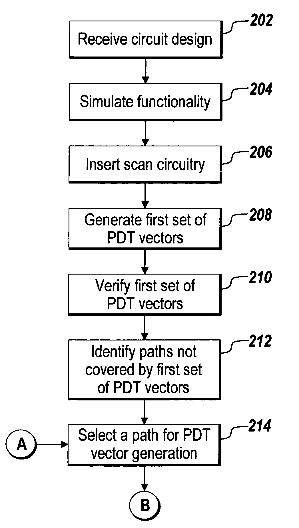
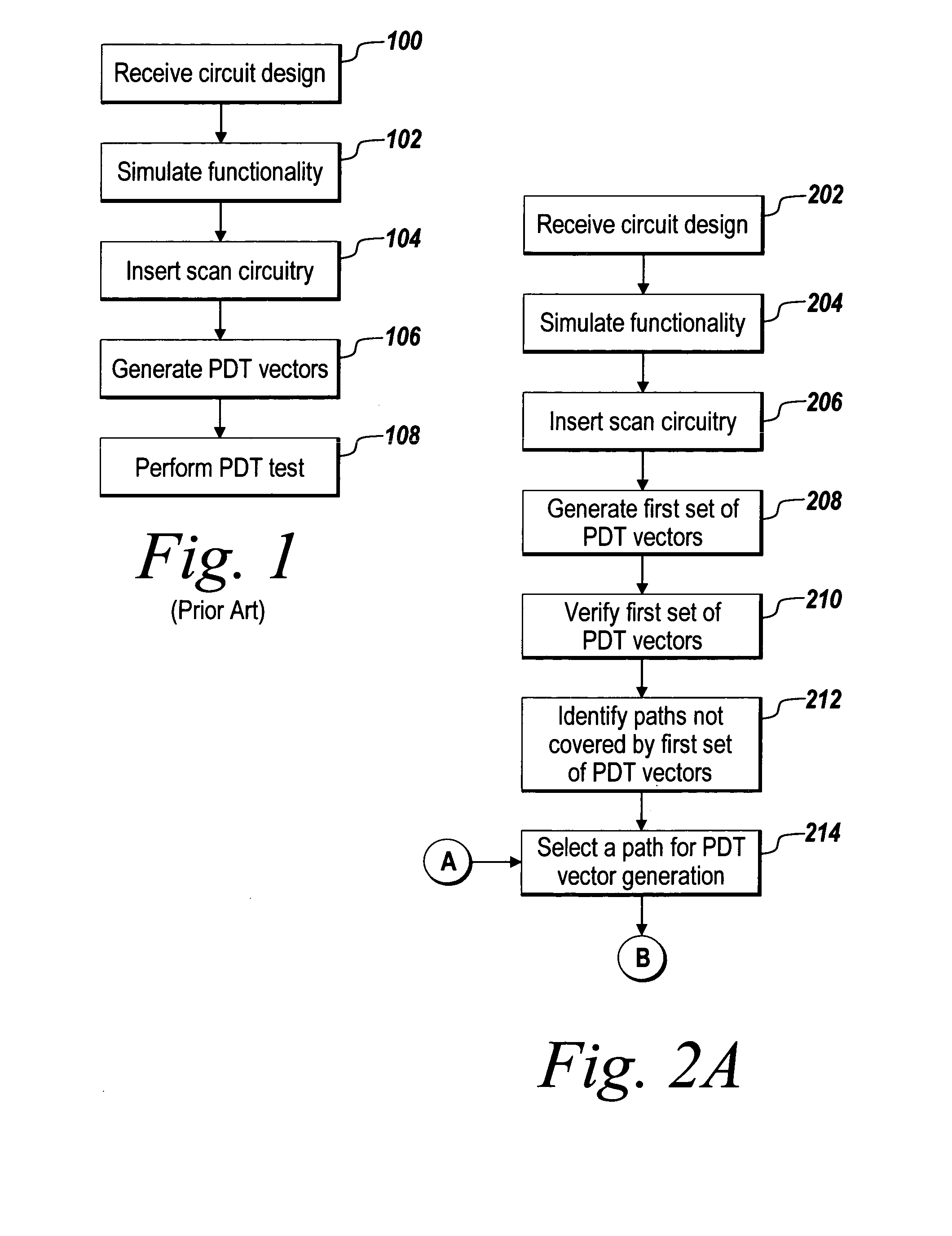
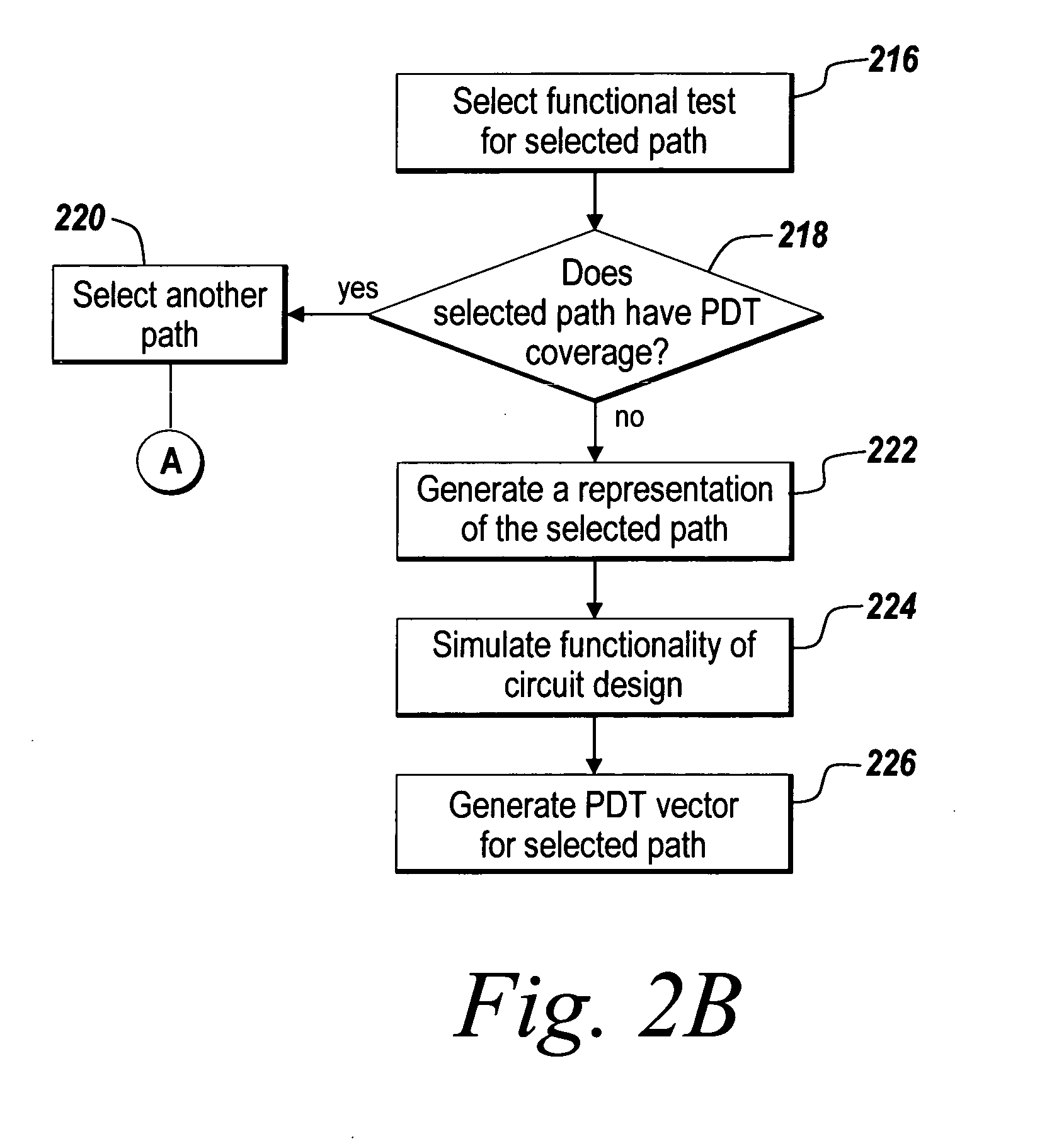
[0008]In one embodiment of the present invention, a method for generating one or more test vectors is disclosed. The method includes the step of performing a functional test on a path having a primary input node and a primary output node. The path is selected from a representation of a circuit design. The method includes the step of performing a structural test on the selected path to detect a functional test state of the primary output node of the selected path, and generating a path delay test vector capable of providing path delay fault coverage for the selected path based on the detected state of the primary output node. The selected path can be free of path delay test coverage.

Problems solved by technology

With the advancement of semiconductor fabrication processes circuit designs continue to grow in size and complexity.
So PDT test vector generation can only be performed successfully on a small portion of paths.
However, functional test generation for an ATE is often time consuming, may or may not be at speed capable, and requires highly specialized pieces of capital equipment.

Method used


Image

  • Method and system for automated path delay test vector generation from functional tests
  • Method and system for automated path delay test vector generation from functional tests
  • Method and system for automated path delay test vector generation from functional tests

Examples


Embodiment Construction

[0025]The illustrative embodiment of the present invention provides methods and a system to increase PDT test coverage for a circuit design and a fabricated representation of the integrated circuit. The methods and system generate PDT test vectors using functional tests (i.e., register transfer level (RTL) functional tests or simulation) and structural tests (i.e., tests that observe the state of internal signals at primary outputs or a sequential logic element). The methods and system disclosed herein can significantly increase PDT test coverage for a circuit design and hence, a fabricated version of the circuit design. Generation of PDT test vectors can be undertaken in an automated manner.

[0026]PDT test coverage may increase 30% or more are realizable by the use and performance of the methods and system disclosed herein. The 30% PDT test coverage increase is compared to the conventional methodology of generating PDT test vectors based on access to test nodes of the circuit design...


PUM


Abstract

Disclosed herein are methods and systems for generating test vectors for use in verification of a circuit design and for hardware testing on a fabricated circuit representative of the circuit design. The system and methods can systematically and automatically perform functional and structural testing on selected paths of the circuit design and, in turn, generate one or more test vectors to increase PDT test coverage using the results of the structural test on the selected path.

Description

TECHNICAL FIELD OF INVENTION[0001]The present invention generally relates to integrated circuits, and more particularly, to the design and fabrication of integrated circuits.BACKGROUND OF THE INVENTION[0002]With the advancement of semiconductor fabrication processes circuit designs continue to grow in size and complexity. As such, the need for comprehensive verification and validation of a circuit design also increases.[0003]Conventionally, the design of an integrated circuit relied on manual development of directed tests and large regressions to find non-compliances in a circuit design. Test plans consistent with test descriptions were used to write a large number of directed tests. These tests were created using a combination of tools and methodologies created by the engineers working on the design.[0004]Recently, a number of business entities, such as Mentor Graphics of Wilsonville, Oreg. and Cadence Design Systems of San Jose, Calif. have developed and marketed a number of tools...

Claims


Application Information

Patent Timeline
Patent Type & Authority Applications(United States)
IPC IPC(8): G01R31/28G06F11/00
CPCG01R31/3016
Inventor WATKINS, DANIELCHEN, LIANG-CHI
Owner ORACLE INT CORP
Why Eureka
Eureka Blog
Learn More