Semiconductor memory device and method for reducing cell activation during write operations

a memory device and memory technology, applied in the field of memory devices for reducing cell activation during write operations, can solve the problems of increasing the current demand for activation and the advantages of conventional art b>2/b> are relatively modes

Active Publication Date: 2008-05-01
SAMSUNG ELECTRONICS CO LTD
View PDF1 Cites 36 Cited by
  • Summary
  • Abstract
  • Description
  • Claims
  • Application Information

AI Technical Summary

Problems solved by technology

One problem with variable resistive semiconductor memory devices and some other memory device types is that activation current demands increase with the number of ...

Method used


Image

  • Semiconductor memory device and method for reducing cell activation during write operations
  • Semiconductor memory device and method for reducing cell activation during write operations
  • Semiconductor memory device and method for reducing cell activation during write operations

Examples


Embodiment Construction

[0024]Embodiments of the present invention now will be described more fully hereinafter with reference to FIGS. 3A to 8, in which embodiments of the invention are shown. This invention may, however, be embodied in many different forms and should not be construed as limited to the embodiments set forth herein. Rather these embodiments are provided so that this disclosure will be thorough and complete, and will fully convey the scope of the invention to those skilled in the art.

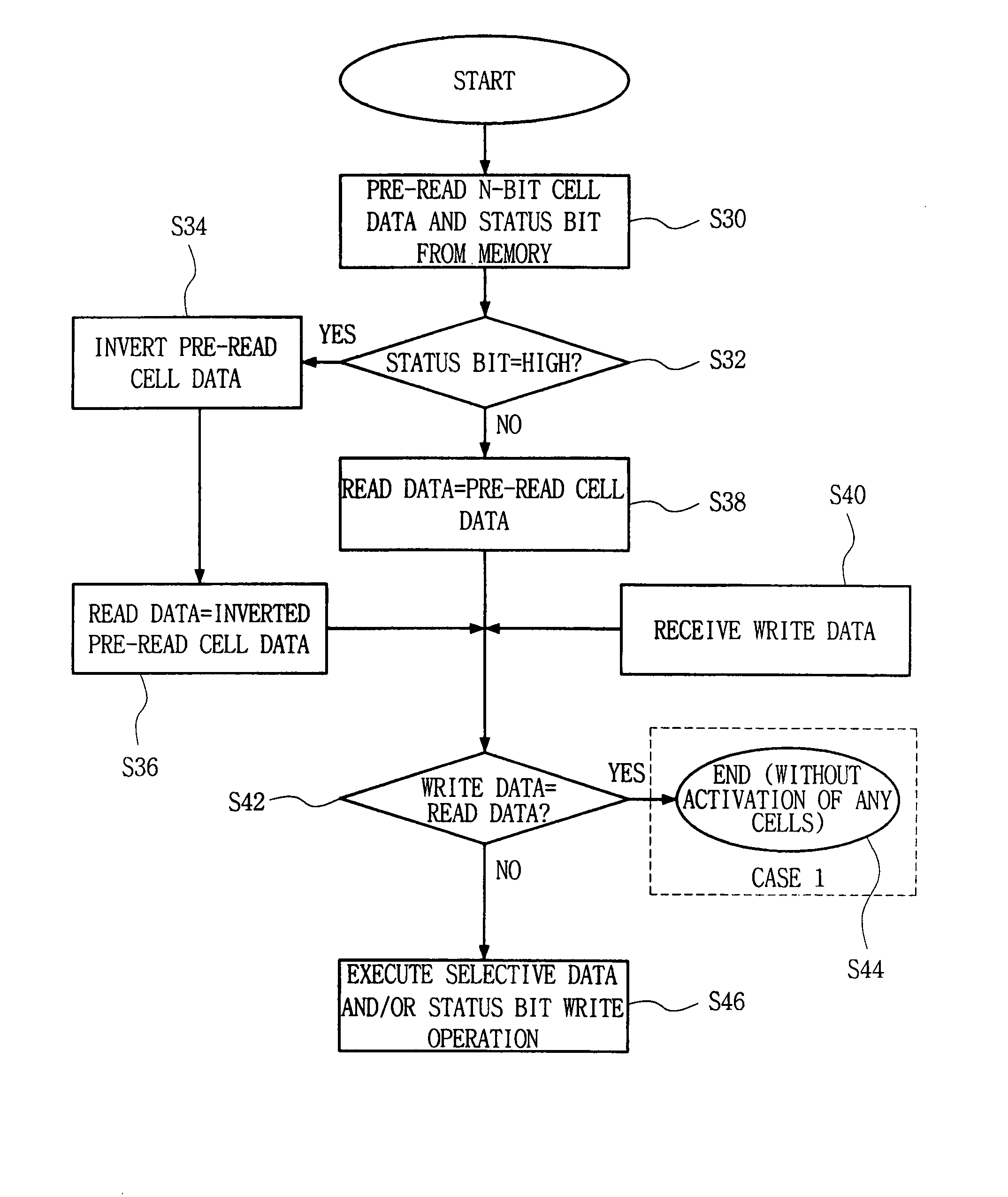
[0025]FIG. 3A is a flowchart for a write operation according to an embodiment of the invention. The process begins by pre-reading N-bit cell data and a status bit from memory in step S30. In conditional step S32, the process determines whether the status bit is high. A high status bit indicates that the stored data bits are inverted. Where the status bit is determined to be high, the process advances to step S34 to invert the pre-read cell data, and then to step S36 where the read data is set equal to the inver...


PUM


Abstract

Embodiments of the invention provide devices or methods that include a status bit representing an inversion of stored data. New data is written to selected cells, the new data is selectively inverted, and the status bit is selectively toggled, based on a comparison between pre-existing data and new data associated with a write command. A benefit of embodiments of the invention is that fewer memory cells must be activated in many instances (when compared to conventional art approaches). Moreover, embodiments of the invention may also reduce the average amount of activation current required to write to variable resistive memory devices and other memory device types.

Description

BACKGROUND AND SUMMARY[0001]1. Field of the Invention[0002]The present invention relates generally to semiconductor memory devices, and more particularly to a device and method for reducing cell activation during write operations.[0003]This application claims priority under 35 U.S.C. §119 from Korean Patent Application 10-2006-0107096, filed on Nov. 1, 2006, the contents of which are hereby incorporated by reference in their entirety for all purposes as if fully set forth herein.[0004]2. Description of the Related Art[0005]There are many types of memory devices. Nonvolatile memory types include variable resistive memory devices such as PRAM (Phase change Random Access Memory) containing phase change material, RRAM (Resistive Random Access Memory) containing material having properties of variable resistance, and an MRAM (Magnetic Random Access Memory) containing ferromagnetic material. Materials forming such memory devices have in common a characteristic that a resistance value is va...

Claims


Application Information

Patent Timeline
IPC IPC(8): G11C7/06
CPCG11C7/06G11C7/1006G11C2211/5647G11C13/0069G11C2013/0076G11C13/0004
Inventor LEE, KWANG-JINKANG, SANG-BEOMOH, HYUNG-ROKCHO, BEAK-HYUNGCHO, WOO-YEONG
Owner SAMSUNG ELECTRONICS CO LTD
Why Eureka
Try Eureka