
Film and chip packaging process using the same

a technology of film and chip, applied in the field of film, can solve the problems of reducing the yield of the chip stacking package, chip cracking, and requiring a higher manufacturing cost and longer packaging time, so as to avoid stress and eliminate the effect of chip crack

Inactive Publication Date: 2008-05-15
ORIENT SEMICON ELECTRONICS
View PDF20 Cites 4 Cited by
  • Summary
  • Abstract
  • Description
  • Claims
  • Application Information

AI Technical Summary

Benefits of technology

[0009] It is an object of the present invention to provide a film and a chip packaging process using the same, wherein the adhesive area between the film and the chip is increased so as to avoid stress increasing after an encapsulating process and further eliminate chip crack.
[0011] It is a further object of the present invention to provide a film and a chip packaging process using the same, which can decrease packaging time by adhering a film on the back surface of a chip rather than smearing adhesive thereon every time before die attach.
[0012] It is a further object of the present invention to provide a film and a chip packaging process using the same, wherein the film has a constant volume and height such that the difficult control problem of the height of the chip during die attach can be overcome so as to increase the manufacturing yields.

Problems solved by technology

However, this chip stacking package requires a higher manufacturing cost and longer packaging time.
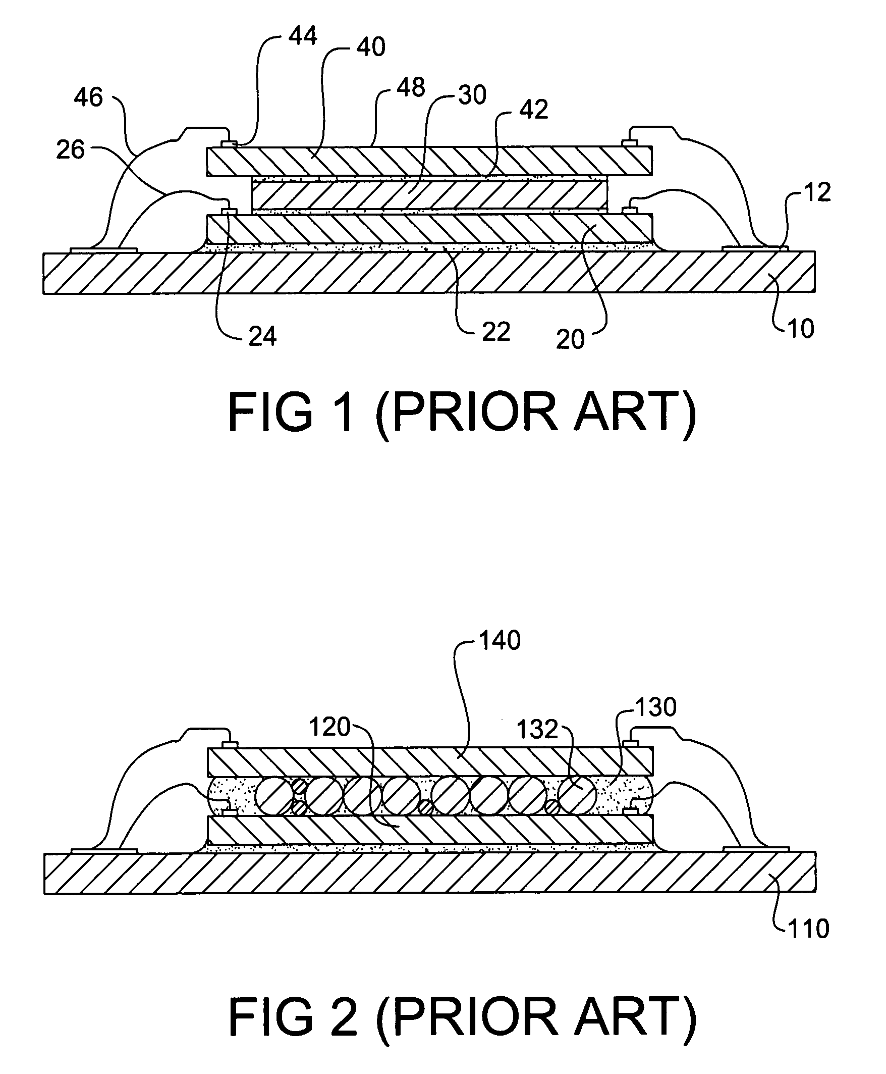
Furthermore, there is a mismatch between the expansion coefficients of the dummy chip and the adhesive, and thus the stress at the interface between the dummy chip and the adhesive is increased after an encapsulating process, thereby further resulting in chip crack and reducing the yield of the chip stacking package.
However, since the partially-cured resin will be melted under heating, the necessary height between the first chip and the substrate (or the second chip) may not able to be maintained if the attaching force during die attach is too high.
The first chip may contact with the bonding wires and thus reduce the yield of the chip stacking package.

Method used


Image

  • Film and chip packaging process using the same
  • Film and chip packaging process using the same
  • Film and chip packaging process using the same

Examples


first embodiment

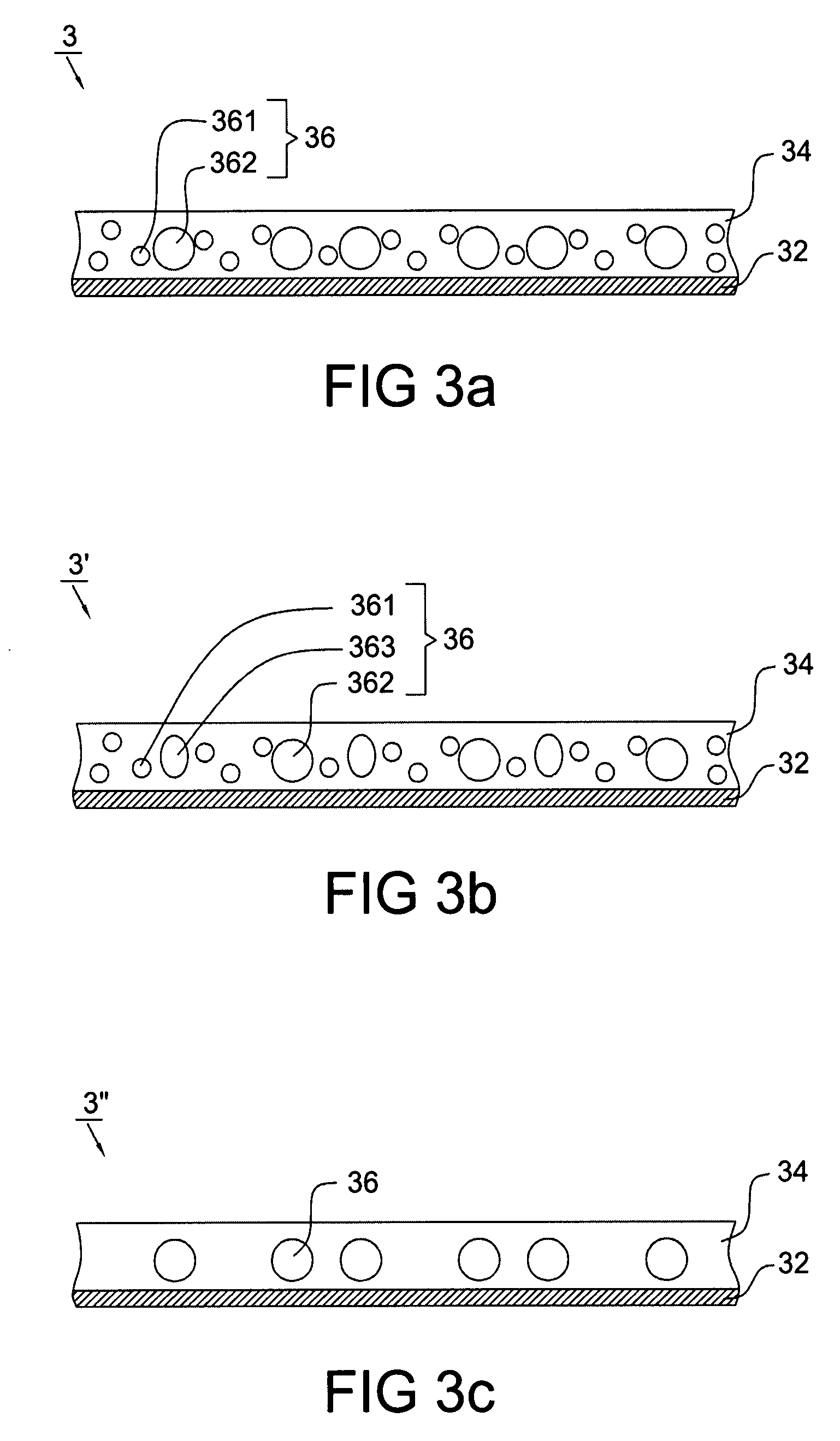
[0025] Referring to FIG. 3a, it shows a film 3 according to the present invention. The film 3 includes a removable base material 32, a resin layer 34 and a plurality of arc elastomers 36 disposed inside the resin layer 34. The film 3 can be utilized in a chip packaging process as an adhesive material for chips. Embodiments of the base material 32 include a BT substrate and a tape. When the base material 32 is a BT substrate, it can be combined to the resin layer 34 by means of an epoxy; on the other hand, when the base material 32 is a tape, e.g. a flexible tape, a UV tape or a blue tape, it can be directly attached to the resin layer 34. A resin layer 34 in the solid state interfused within the arc elastomers 36 is adhered to the base material 32. In order to be adapted to chip packaging processes, the base material 32 preferably can endure at least a temperature of 85 degrees centigrade.

[0026] One embodiment of the resin layer 34 is a partially-cured resin, e.g. a resin composed o...

second embodiment

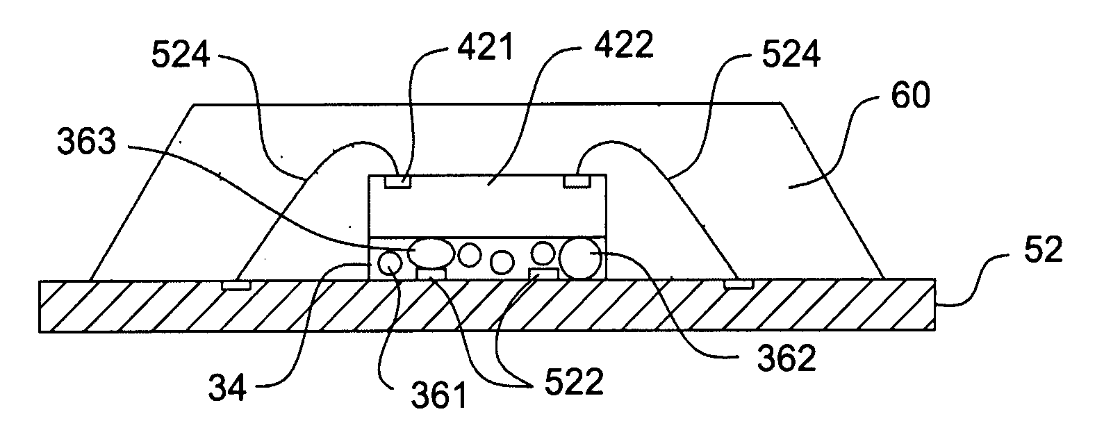
[0034] Referring to FIG. 5e, the first chip 422 is then mounted on a carrier 52 through the film 3′ (step 205). In the embodiment of the present invention, the carrier 52 can be a substrate, a lead frame or a chip (a second chip). In order to have the first chip 422 to be adhered to the carrier 52 through the resin layer 34, the first chip 422 has to be heated to a relatively high temperature for a short period of time, e.g. higher than 85 degrees centigrade for 2 seconds, such that the first chip 422 can be pre-adhered to the carrier 52. If the carrier 52 is a substrate, it is preferably to use the film 3′ of the second embodiment as an adhesive material for the adhesion of the first chip 422, wherein the arc elastomers 36 are classified into a plurality of first balls 362, second balls 361 and spheroids 363 and the first balls 362 and the spheroids 363 are separated by the second balls 361. When the resin layer 34 is adhered to the carrier 52, due to the resin layer 34 appearing h...


PUM

PropertyMeasurementUnit
heightaaaaaaaaaa
temperatureaaaaaaaaaa
temperaturesaaaaaaaaaa

Abstract

A film includes a removable base material, a resin layer and a plurality of arc elastomers. The resin layer is a partially-cured resin which is in a half-melting state with viscosity at a temperature higher than a first temperature and in a solid state without viscosity at a temperature lower than a second temperature, and the resin layer in a solid state is adhered on the base material. The arc elastomers are disposed inside the resin layer. The present invention further provides a chip packaging process using the film.

Description

CROSS REFERENCE TO RELATED APPLICATION [0001] This application claims the priority benefit of Taiwan Patent Application Serial Number 095141502, filed on Nov. 9, 2006, the full disclosure of which is incorporated herein by reference. BACKGROUND OF THE INVENTION [0002] 1. Field of the Invention [0003] This invention generally relates to a film, and more particularly, to a film utilized in a chip packaging process. [0004] 2. Description of the Related Art [0005] In a conventional chip stacking package, as shown in FIG. 1, the package includes a substrate 10, a lower chip 20, a dummy chip 30 and an upper chip 40. The lower chip 20 is mounted on the substrate 10 by means of an adhesive 22, and two side edges of the upper surface of the lower chip 20 are provided with a plurality of aluminum pads 24 which are electrically connected to a plurality of pads 12 of the substrate 10 through a plurality of first bonding wires 26. The dummy chip 30 is mounted on the lower chip 20 by means of an ...

Claims


Application Information

Patent Timeline
Patent Type & Authority Applications(United States)
IPC IPC(8): H01L21/58B32B5/16B32B7/12
CPCH01L2224/2929H01L2224/293H01L21/6835H01L24/27H01L24/29H01L24/83H01L24/85H01L25/50H01L2224/05624H01L2224/274H01L2224/27436H01L2224/29198H01L2224/32145H01L2224/32225H01L2224/48091H01L2224/48227H01L2224/48247H01L2224/73265H01L2224/83191H01L2224/83856H01L2225/0651H01L2225/06572H01L2924/01005H01L2924/01013H01L2924/01082H01L2924/07802H01L2924/19015H01L2924/19103H01L2224/2919H01L2924/01006H01L2924/01033H01L2924/0665H01L2224/85H01L2224/83139Y10T428/28Y10T428/25H01L2924/00014H01L2924/00H01L2924/3512H01L2924/00012H01L2924/181H01L24/73H01L24/48H01L2224/45015H01L2924/207H01L2224/45099H01L23/48H01L23/12
Inventor TUNG, YUEH MINGSUN, KUO YANGYANG, CHIA MINGMAI, HUNG TAILIU, HUI CHI
Owner ORIENT SEMICON ELECTRONICS
Learn More