Mugfet with increased thermal mass

a technology of thermal mass and mugfet, which is applied in the direction of semiconductor devices, semiconductor/solid-state device details, electrical devices, etc., can solve the problems of poor thermal capacity, extreme heating and possible damage to the device, and extreme rise in temperatur

Active Publication Date: 2008-05-22
INFINEON TECH AG
View PDF8 Cites 52 Cited by
  • Summary
  • Abstract
  • Description
  • Claims
  • Application Information

AI Technical Summary

Benefits of technology

[0035]Such embodiments of the inventive subject matter may be referred to herein, individually and / or collectively, by the term “invention” merely for convenience and without intending to voluntarily limit the scope of this application to any single invention or inventive concept if more than one is in fact disclosed. Thus, although specific embodiments have been illustrated and described herein, it should be appreciated that any arrangement calculated to achieve the same purpose may be substituted for the specific embodiments shown. This disclosure is intended to cover any and all adaptations or variations of various embodiments. Combinations of the above embodiments, and other embodiments not specifically described herein, will be apparent to those of skill in the art upon reviewing the above description.

Problems solved by technology

Multigate (MuGFET) or FinFET devices are expected to be used in the future due to the difficulty of further down-scaling of bulk CMOS technologies.
Because some low-cost embodiments of MuGFET manufacturing processes result in embodiments where the fin region 18 is largely devoid of deposited silicon, the relatively low thermal mass of the very thin fin region 18 results in extreme heating and possible damage to the device if an electrostatic event causes a large transient current flow, and an extreme rise in temperature in the channel of fin 18.
In MuGFET devices the buried oxide layer blocks the flow of heat to the substrate because of poor thermal capacity and poor thermal conductivity of the insulating material such as SiO2.

Method used


Image

  • Mugfet with increased thermal mass
  • Mugfet with increased thermal mass
  • Mugfet with increased thermal mass

Examples


Embodiment Construction

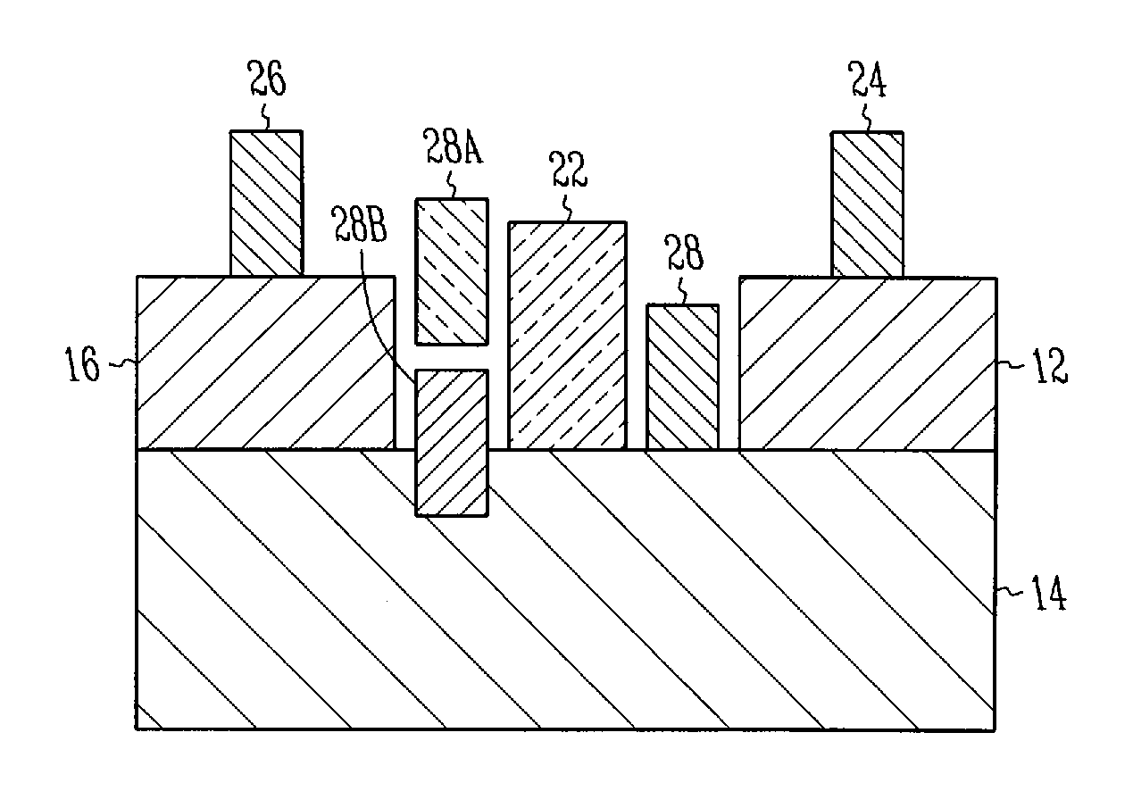
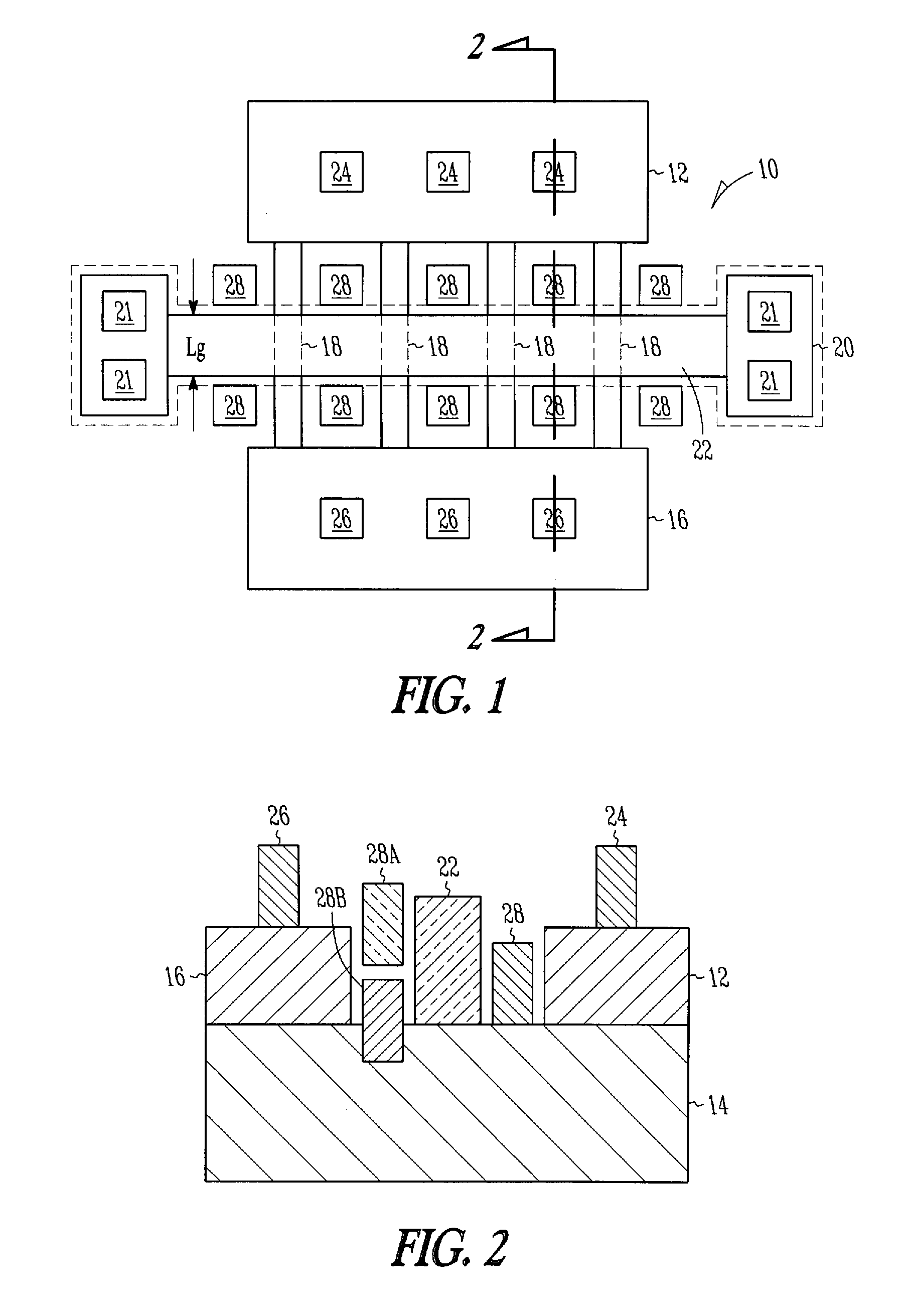
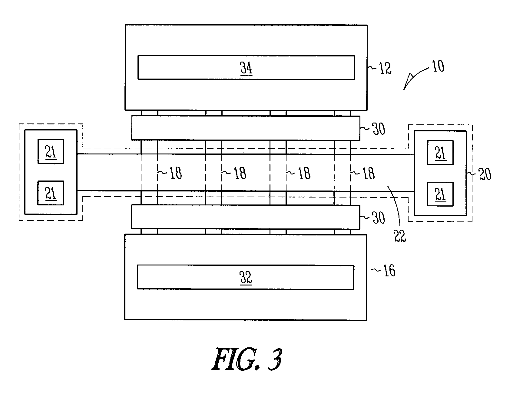
[0015]Many of the various disclosed embodiments relate to semiconductor devices and methods of fabricating such devices, and in particular to MuGFETs or FinFETs. Specific details of certain embodiments of the invention are set forth in the following description and in FIGS. 1 through 12 to provide a thorough understanding of such embodiments. One skilled in the art, however, will understand that other embodiments are possible, and that many embodiments may be practiced without several of the details described herein.

[0016]FIGS. 1 and 2 illustrate a semiconductor device 10 according to some embodiments of the invention. In some embodiments, semiconductor device 10 is a MuGFET (a multiple gate field effect transistor) device. In some embodiments, semiconductor device 10 is a MuGFET ESD (electrostatic discharge) protective device. In some embodiments, semiconductor device 10 is an I / O device.

[0017]FIG. 1 shows the layout of device 10. In some embodiments, device 10 is a Silicon-on-insu...


PUM


Abstract

Some embodiments discussed herein include a semiconductor having a source region, a drain region and an array of fins operatively coupled to a gate region controlling current flow through the fins between the source region and the drain region. The semiconductor also has at least one cooling element formed at least in part of a material having a heat capacity equal to or larger than the heat capacity of the material of the source region, drain region and array of fins, the cooling elements being in close vicinity to fins of the array of fins electrically isolated from the fins of the array, the source region and the drain region. Other embodiments are also disclosed

Description

TECHNICAL FIELD[0001]The information disclosed herein relates generally to integrated circuit devices and fabrication methods, including semiconductor devices and methods of forming such devices.BACKGROUND[0002]Multigate (MuGFET) or FinFET devices are expected to be used in the future due to the difficulty of further down-scaling of bulk CMOS technologies. Such devices may typically be designed for high-speed logic core applications with low supply voltages. It is necessary for such devices to be able to operate following Electrostatic Discharge (ESD) events.BRIEF DESCRIPTION OF THE DRAWINGS[0003]FIG. 1 is a top view of some embodiments of the invention showing dummy contacts as cooling elements in the open space between fins;[0004]FIG. 2 is a cross sectional view taken along lines 2-2′ of FIG. 1;[0005]FIG. 3 is a top view of some embodiments of the invention showing dummy bar contacts as cooling elements formed above the fins;[0006]FIG. 4 is a top view of some embodiments of the in...

Claims


Application Information

Patent Timeline
Patent Type & Authority Applications(United States)
IPC IPC(8): H01L29/786H01L21/336
CPCH01L23/367H01L27/0248H01L29/66795H01L29/785H01L2924/0002H01L2924/00
Inventor GOSSNER, HARALDRUSS, CHRISTIANSCHNEIDER, JENSSCHULZ, THOMAS
Owner INFINEON TECH AG
Why Eureka
Try Eureka