Heat spreader for a multi-chip package

a multi-chip package and heat spreader technology, applied in the direction of semiconductor devices, semiconductor/solid-state device details, electrical apparatus, etc., can solve the problems of device failure, reliability and performance deficiencies, and mismatches in the coefficient of thermal expansion (cte)

Inactive Publication Date: 2008-06-05
INTEL CORP
View PDF8 Cites 88 Cited by
  • Summary
  • Abstract
  • Description
  • Claims
  • Application Information

AI Technical Summary

Problems solved by technology

One challenge facing multi-chip package designers is cooling these devices during operation.
A failure to adequately remove heat from a multi-chip package during operation may lead to reliability and performance deficiencies, and perhaps device failure.
Issues that may arise in designing a cooling solution for a multi-chip package include mismatches in the coefficient of thermal exp

Method used


Image

  • Heat spreader for a multi-chip package
  • Heat spreader for a multi-chip package
  • Heat spreader for a multi-chip package

Examples


Embodiment Construction

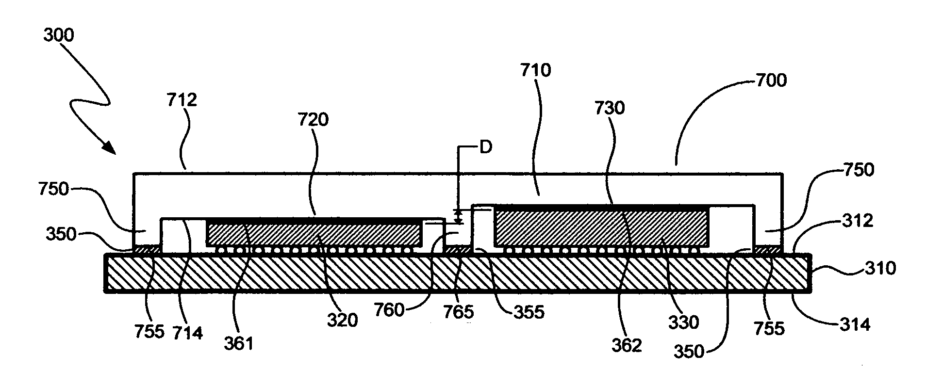
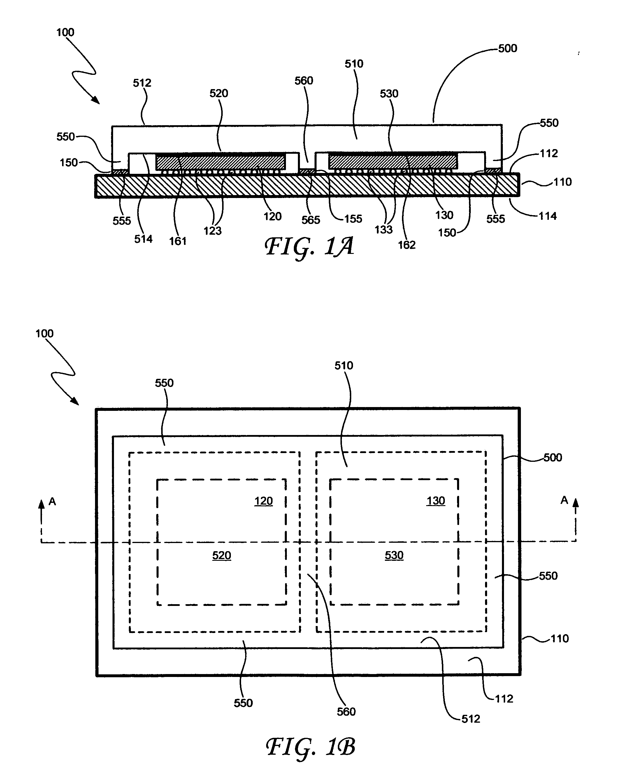
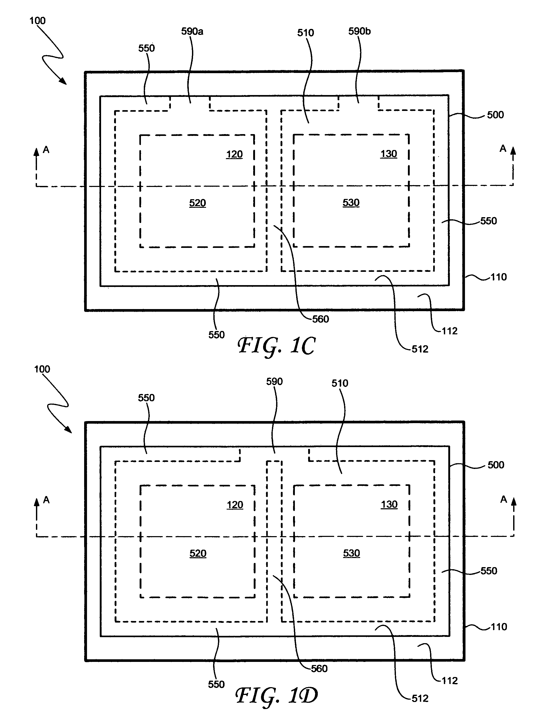
[0009]Referring to FIGS. 1A and 1B, illustrated is a multi-chip package 100. A plan view of the multi-chip package 100 is shown in FIG. 1B, whereas a cross-sectional elevation view of the package 100, as taken along line A-A of FIG. B, is shown in FIG. 1A. The multi-chip package 100 includes a substrate 110, a first integrated circuit (IC) die 120, a second IC die 130, and an embodiment of a heat spreader 500. The heat spreader 500 includes a member (e.g., a wall) extending between the heat spreader's body and the underlying substrate 110, and this member can stiffen the package and reduce warpage of the substrate 110. By reducing substrate warpage, the heat spreader 500 may assist in minimizing failures, such as thermal interface delamination, which can lead to improved reliability. Embodiments of this heat spreader are described in greater detail below.

[0010]The substrate 110 may comprise any suitable type of package substrate or other die carrier. In one embodiment, the substrate...


PUM


Abstract

Embodiments of a heat spreader and an assembly including such a heat spreader are disclosed. The heat spreader includes a stiffening member, which in one embodiment comprises a wall extending from a lower surface of the heat spreader. The wall may be coupled with a substrate, and the addition of this wall may decrease warpage of the substrate and increase package stiffness. The wall may be located between adjacent integrated circuit die that are disposed on the substrate. Other embodiments are described and claimed.

Description

FIELD OF THE INVENTION[0001]The disclosed embodiments relate generally to the cooling of integrated circuit (IC) devices, and more particularly to a heat spreader for use in multi-chip packages.BACKGROUND OF THE INVENTION[0002]Multi-chip assemblies can provide greater integration and enhanced function in a single package. Integration of IC devices fabricated by different process flows into a single package is possible, and can pave the way for system-in-package (SIP) solutions. In addition to the aforementioned benefits, these SIP or multi-chip packages may exhibit reduced form factors, perhaps including both a smaller overall height as well as a smaller footprint—e.g., the surface area occupied by the package on a next-level component, such as a circuit board—as compared to a similar system having multiple, separate components mounted on a circuit board or other substrate.[0003]One challenge facing multi-chip package designers is cooling these devices during operation. Heat removal...

Claims


Application Information

Patent Timeline
IPC IPC(8): H01L23/34
CPCH01L23/10H01L23/3675H01L23/3737H01L23/42H01L25/0655H01L2224/16225H01L2924/1433H01L2924/1461H01L2924/01019H01L2224/32245H01L2224/73253H01L2924/16153H01L2924/00H01L2924/00014H01L2924/00011H01L2224/0401
Inventor CHAO, TONG WA
Owner INTEL CORP
Why Eureka
Try Eureka