Unlock instant, AI-driven research and patent intelligence for your innovation.

Memory cell, erasing method of information recorded in the memory cell, and nonvolatile semiconductor memory device comprising the memory cell

a technology of memory cells and erasing methods, which is applied in the field of memory cells, can solve the problems of lowering the reliability of electric charge retention, the difficulty of implementing the above process in the standard cmos manufacturing process without adding a new step, etc., and achieves the effect of satisfying programming, reading, and erasing abilities

Inactive Publication Date: 2008-06-05
SHARP KK
View PDF24 Cites 14 Cited by
  • Summary
  • Abstract
  • Description
  • Claims
  • Application Information

AI Technical Summary

Benefits of technology

[0027]The present invention was made in view of the above problems and it is an object of the present invention to provide a nonvolatile memory cell that can be mounted in a CMOS manufacturing process, and is capable of implementing high level of programming, reading and erasing ability. The present invention also relates to an erasing method of information recorded in the memory cell and a nonvolatile semiconductor memory device comprising a plurality of the memory cells.

Problems solved by technology

Conversely, in order to increase the withstand voltage of the N-type impurity diffusion layer 9, it is necessary to correct an impurity density distribution of the N-type impurity diffusion layer 9, so that it is difficult to implement the above process in the standard CMOS manufacturing process without adding a new step.
However, in this method, the electrons accumulated in the floating gate electrode FG after the programming process could escape through the thin insulation film (corresponding to the above-described extremely thin gate insulation film) even though the erasing action is not performed (electric charge retention reliability is lowered).

Method used


Image

  • Memory cell, erasing method of information recorded in the memory cell, and nonvolatile semiconductor memory device comprising the memory cell
  • Memory cell, erasing method of information recorded in the memory cell, and nonvolatile semiconductor memory device comprising the memory cell
  • Memory cell, erasing method of information recorded in the memory cell, and nonvolatile semiconductor memory device comprising the memory cell

Examples


Embodiment Construction

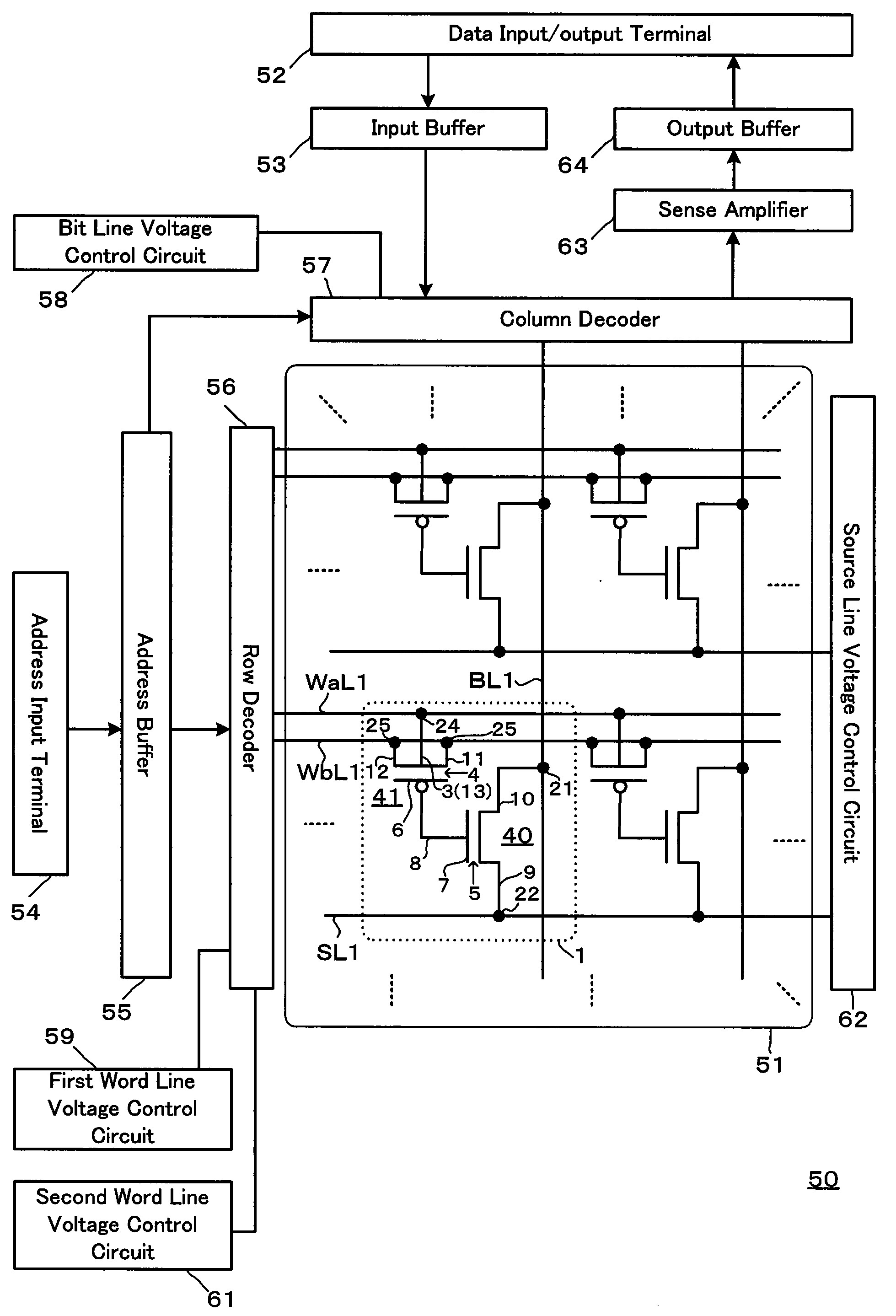
[0077]An embodiment of a memory cell according to the present invention (referred to as the “memory cell of the present invention” occasionally hereinafter), an erasing method of information recorded in the memory cell of the present invention (referred to as the “method of the present invention” occasionally hereinafter), and a nonvolatile semiconductor memory device comprising the memory cell of the present invention (referred to as the “device of the present invention” occasionally hereinafter) will be described with reference to FIGS. 1 to 11. First, a description will be made of a constitution example of the whole device of the present invention and then a description will be made of a constitution and a layout of the memory cell of the present invention.

Description of Device of the Present Invention

[0078]FIG. 1 is a block diagram showing the whole schematic constitution of the nonvolatile semiconductor memory device of the present invention. As shown in FIG. 1, a device 50 of ...


PUM


Abstract

A nonvolatile memory cell that can be mounted in a CMOS manufacturing process, and is capable of implementing high level of programming, reading and erasing ability. The memory cell is configured by a MOS transistor comprising two N-type first impurity diffusion layers formed separately on a P-type semiconductor substrate, and a first gate electrode formed above a first cannel region sandwiched by both diffusion layers through a first gate insulation film, a first capacitor comprising P-type second impurity diffusion layers formed on a well, and a second gate electrode formed above the diffusion layer through a second gate insulation film, and a second capacitor comprising the well adjacent to the second impurity diffusion layer, and a third gate electrode formed above the well through a third gate insulation film, wherein a different voltage can be applied to each of the capacitors.

Description

CROSS REFERENCE TO RELATED APPLICATION[0001]This Nonprovisional application claims priority under 35 U.S.C. § 119(a) on Patent Application No. 2006-305230 filed in Japan on 10 Nov., 2006 and Patent Application No. 2007-080280 filed in Japan on 26 Mar., 2007 the entire contents of which are hereby incorporated by reference.BACKGROUND OF THE INVENTION[0002]1. Field of the Invention[0003]The present invention relates to a memory cell and more particularly, to a memory cell that can be mounted on a substrate in a standard CMOS process and written with information electrically. In addition, the present invention relates to an erasing method of information recorded in the memory cell and a nonvolatile semiconductor memory device comprising the plurality of memory cells.[0004]2. Description of the Related Art[0005]Conventionally, there is provided a nonvolatile semiconductor memory device that can be provided in the standard CMOS process without adding a new process to the process and writ...

Claims


Application Information

Patent Timeline
IPC IPC(8): G11C11/34H01L27/115
CPCG11C8/10G11C16/10H01L27/11558H01L27/115H01L27/11521G11C2216/10H10B69/00H10B41/60H10B41/30
Inventor UEDA, NAOKIYAMAUCHI, YOSHIMITSU
Owner SHARP KK