Eureka AIR delivers breakthrough ideas for toughest innovation challenges, trusted by R&D personnel around the world.

Nanostructure optical insulating membrane

a technology of optical insulation membrane and nanostructure, which is applied in the field of nanostructure optical insulation membrane, can solve the problems of reducing the visible light transmission rate to 20-70%, disadvantaged buildings equipped with insulating membranes, and complex manufacturing process, so as to improve the visible light transmission rate and reduce internal reflection

Inactive Publication Date: 2008-06-26
IND TECH RES INST
View PDF7 Cites 6 Cited by
  • Summary
  • Abstract
  • Description
  • Claims
  • Application Information

AI Technical Summary

Benefits of technology

[0008]It is a primary objective of the present invention to disclose a nanostructure optical insulating membrane adapted to provide thermal insulation, enhance illumination, and enable users to see farther.
[0011]Unlike the prior art, the prevent invention discloses a nanostructure optical insulating membrane that, upon exposure to light, enhances visible light transmission, reduces internal reflection, provides thermal insulation by blocking infrared light by means of a metal layer, and enables users to see farther.

Problems solved by technology

Hence, the fabrication process is complex and expensive.
More badly, an insulating membrane that comprises one or more metal layers decreases visible light transmission to 20-70%, which is an inevitable drawback of the prior art.
A building equipped with insulating membranes is disadvantaged by poor illumination and excessive internal reflection.
Owing to insulating membrane-induced internal reflection, people looking out of a window of the building cannot have a clear view of the outside, that is, they are unable to see farther.
The driver of a vehicle equipped with insulating membranes is denied access to images in rear view mirrors and therefore likely to end up in a traffic accident.
Accordingly, an issue calling for an immediate solution involves developing a nanostructure optical insulating membrane that overcomes the aforesaid drawbacks of the prior art.

Method used


Image

  • Nanostructure optical insulating membrane
  • Nanostructure optical insulating membrane
  • Nanostructure optical insulating membrane

Examples


Embodiment Construction

[0020]The following specific embodiments are provided to illustrate the present invention. Persons skilled in the art can readily gain an insight into other advantages and features of the present invention based on the contents disclosed in this specification.

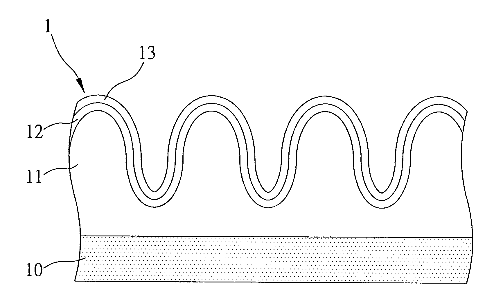
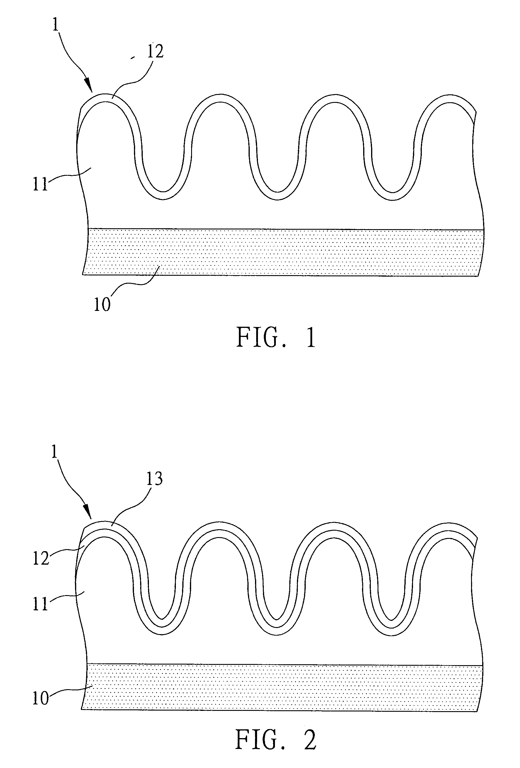
[0021]Referring to FIG. 1, which is a cross-sectional view showing the first embodiment of a portion of a nanostructure optical insulating membrane of the present invention, a nanostructure optical insulating membrane 1 is used in any venues that need thermal insulation, such as indoor environments and vehicles. As shown in the drawing, the nanostructure optical insulating membrane 1 comprises a substrate 10, a nanostructure layer 11, and a metal layer 12.

[0022]The constituent parts of the nanostructure optical insulating membrane 1 of the present invention are described in detail as follows.

[0023]The drawing illustrates the substrate 10 but is not intended to limit the dimensions of the substrate 10. In practice, the dimension...


PUM

PropertyMeasurementUnit
heightaaaaaaaaaa
heightaaaaaaaaaa
thicknessaaaaaaaaaa

Abstract

A nano-structure optical insulating membrane includes a substrate, a nano-structure layer formed on the substrate, and a metal layer formed on the nano-structure layer is disclosed. Upon exposure to light, the nano-structure layer increases visible light transmission but reduces internal reflection, and the metal layer blocks infrared light and thereby provides thermal insulation. The nano-structure optical insulating membrane of the present invention enhances illumination, spares lighting equipment, saves energy, and enables users to see farther.

Description

BACKGROUND OF THE INVENTION[0001]1. Field of the Invention[0002]The present invention relates to nanostructure optical insulating membranes, and more particularly, to a nanostructure optical insulating membrane adapted to provide thermal insulation, enhance illumination, spare lighting equipment, and enable users to see farther.[0003]2. Description of the Prior Art[0004]Insulating membranes are typically used in vehicles and buildings to block UV light and infrared light. Insulating membranes not only block incoming light rays which may harm the human body and damage furniture / fixtures, but also decrease indoor temperature which can otherwise increase because of exposure to unblocked sunlight, thereby making insulating membranes a good energy-saving means.[0005]Insulating membranes currently available on the market block more than 99% of UV light and 35% to 97% of infrared light. An insulating membrane fabrication process is usually based on multi-coating technology, producing optic...

Claims


Application Information

Patent Timeline
Patent Type & Authority Applications(United States)
IPC IPC(8): B32B5/14B23B9/00B32B17/06
CPCB82Y20/00G02B5/282Y10T428/26Y10T428/269Y10T428/256
Inventor TING, CHIA-JENHSU, CHIN-JUNIEH, YA-YUCHOU, CHANG-PIN
Owner IND TECH RES INST
Why Eureka
Eureka Blog
Learn More