Semiconductor memory device and method for driving the same

Active Publication Date: 2008-07-10
SK HYNIX INC
View PDF8 Cites 5 Cited by
  • Summary
  • Abstract
  • Description
  • Claims
  • Application Information

AI Technical Summary

Benefits of technology

[0011]Embodiments of the present invention are directed at providing a semiconductor memor

Problems solved by technology

As semiconductor integrated circuit (IC) technologies are rapidly developed, the operating speed of the data processor increases, but the data input/output speed of the semiconductor memory device does not keep up with the increased operating speed of the data processor.
However, because even the synchronous memory device could not keep up with the operating speed o

Method used


Image

  • Semiconductor memory device and method for driving the same
  • Semiconductor memory device and method for driving the same
  • Semiconductor memory device and method for driving the same

Examples


Embodiment Construction

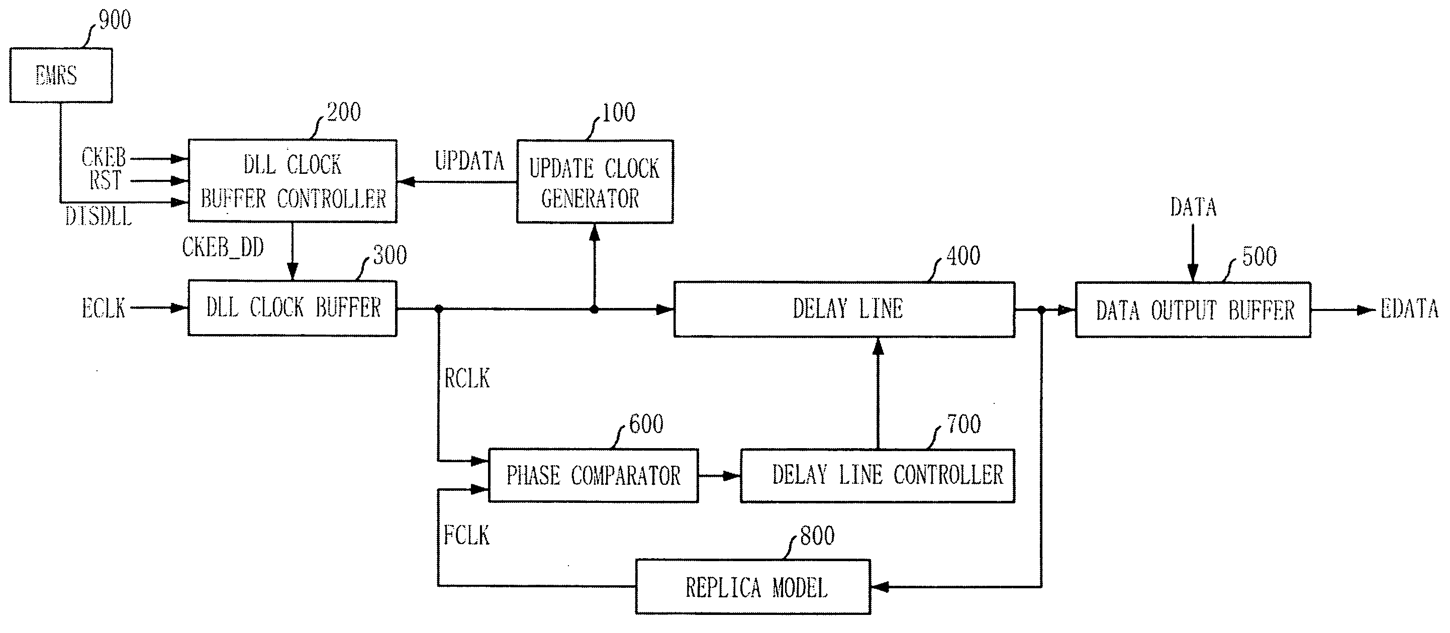
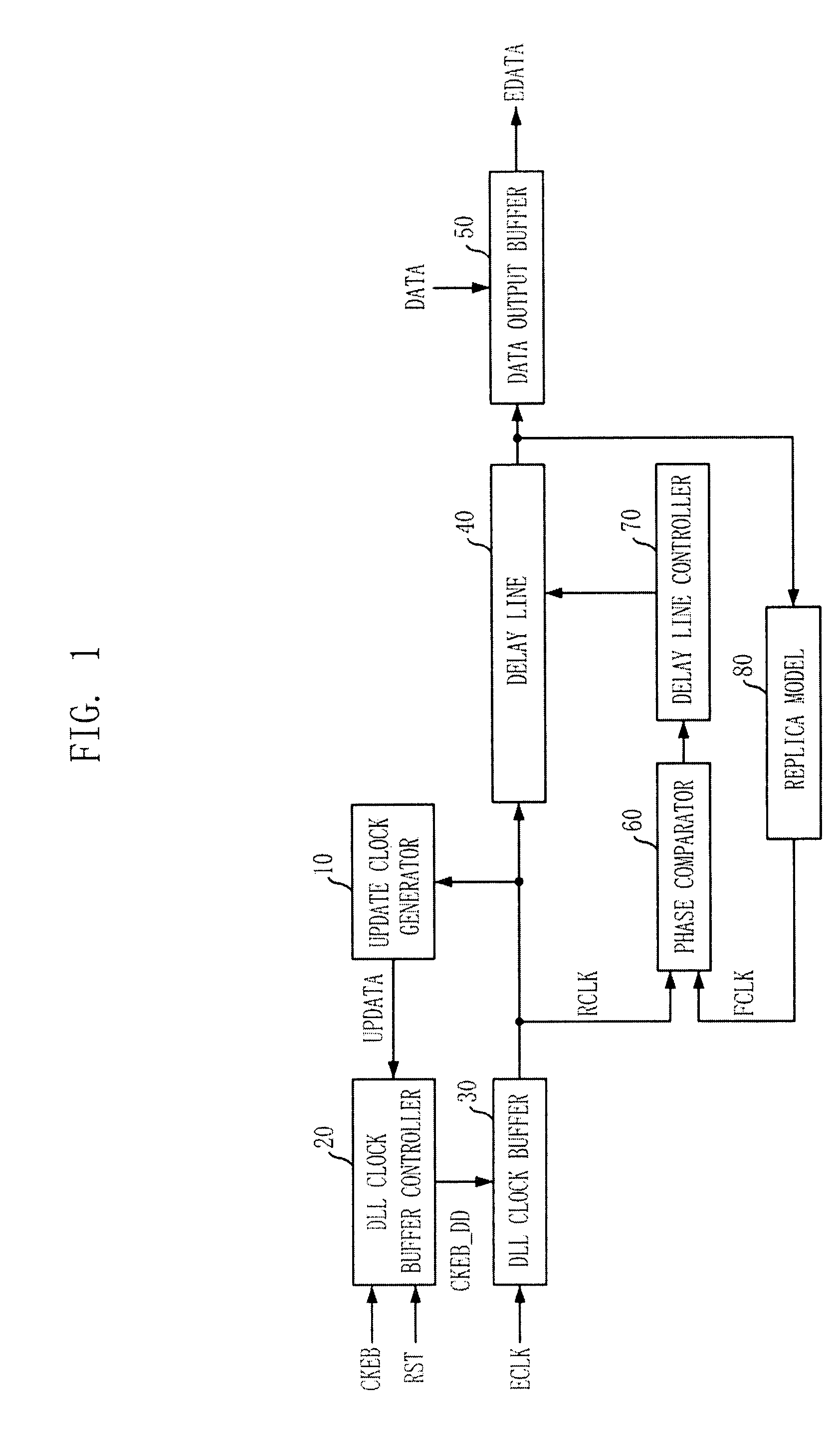
[0020]FIG. 1 is a block diagram of a delay locked loop (DLL) circuit of a semiconductor memory device.

[0021]Referring to FIG. 1, the semiconductor memory device includes an update clock generator 10, a DLL clock buffer controller 20, a DLL clock buffer 30, a delay line 40, a data output buffer 50, a phase comparator 60, a delay line controller 70, and a replica model 80.

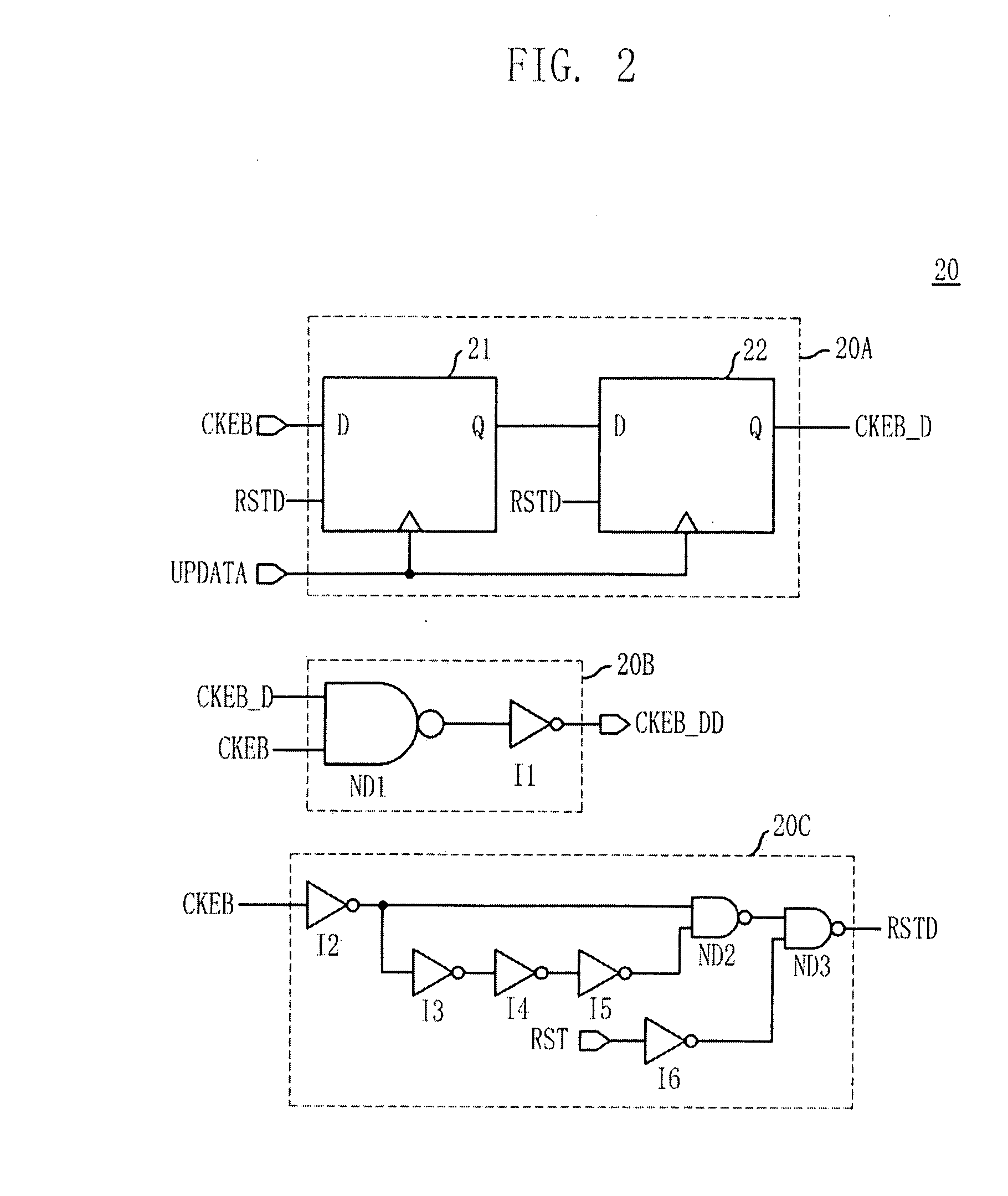
[0022]The update clock generator 10 receives an external system clock ECLK to generate an update clock UPDATE. The update clock UPDATE has half period of the external system clock ECLK and is clocked one time in every 11 periods of the external system clock ECLK. The DLL clock buffer controller 20 receives a clock enable signal CKEB to generate an enable signal CKEB_DD in synchronization with the update clock UPDATE. The DLL clock buffer controller 20 is reset by a reset signal RST. The DLL clock buffer 30 receives the external system clock ECLK to generate a reference clock RCLK.

[0023]The delay line 40 delays the re...


PUM


Abstract

A semiconductor memory device includes: a delay locked loop (DLL) clock buffer for buffering a system clock in response to the a buffer enable signal; a DLL circuit for generating a delay locked loop (DLL) clock by performing a delay locking operation using the buffered system clock; and a DLL clock buffer controller for generating the buffer enable signal in response to a code signal and a clock enable signal, the code signal containing information about whether to perform the delay locking operation.

Description

CROSS-REFERENCE TO RELATED APPLICATIONS[0001]The present invention claims priority of Korean patent application number 10-2007-0002897, filed on Jan. 10, 2007, which is incorporated by reference in its entirety.BACKGROUND OF THE INVENTION[0002]The present invention relates to a semiconductor memory device, and more particularly, to a delay locked loop (DLL) circuit of a semiconductor memory device.[0003]A system is implemented with a plurality of semiconductor devices. Among them, a semiconductor memory device is used to store data. The semiconductor memory device outputs data corresponding to addresses received from a data processor, e.g., a central processing unit (CPU), or stores data received from the data processor into unit cells corresponding to addresses inputted together with the data.[0004]As the operating speed of the system is increasing, the data processor requires the semiconductor memory device to input / output data at higher speed. As semiconductor integrated circuit ...

Claims


Application Information

Patent Timeline
IPC IPC(8): G11C5/14
CPCG11C7/222G11C7/22G11C7/1072H03L7/0812G11C2207/2227
Inventor KIM, KYOUNG-NAMKU, YOUNG-JUNCHOI, HOON
Owner SK HYNIX INC
Why Eureka
Try Eureka