Solid-state imaging device and image capture apparatus

a technology of image capture apparatus and imaging device, which is applied in the field of solid-state imaging device and image capture apparatus, can solve problems such as blooming and achieve the effect of eradicating blooming

Inactive Publication Date: 2008-08-14
SONY CORP
View PDF4 Cites 26 Cited by
  • Summary
  • Abstract
  • Description
  • Claims
  • Application Information

AI Technical Summary

Benefits of technology

[0025]Here, by applying a pre-shutter pulse to pixels belonging to at least a single row or a single column within a succeeding group and adjacent to a preceding group, prior to a shutter pulse, before a reading timing for the preceding group to sweep out unnecessary charges stored in the pixels, it is possible to eliminate blooming or to make blooming amounts from vertically or horizontally adjacent pixels substantially equal for pixels belonging to a group from which signal charges are stored.

Problems solved by technology

By the way, it is generally known that, when light incident onto the image sensor is extremely intense, a phenomenon called blooming occurs due to excessively produced signal charges overflowing and leaking from pixels into adjacent pixels.

Method used


Image

  • Solid-state imaging device and image capture apparatus
  • Solid-state imaging device and image capture apparatus
  • Solid-state imaging device and image capture apparatus

Examples


Embodiment Construction

[0036]An embodiment of the present invention will be described below with reference to the drawings for an understanding of the present invention. It is noted that a pixel circuit structure of a solid-state imaging device according to an embodiment of the present invention is similar to that of the related-art solid-state imaging device.

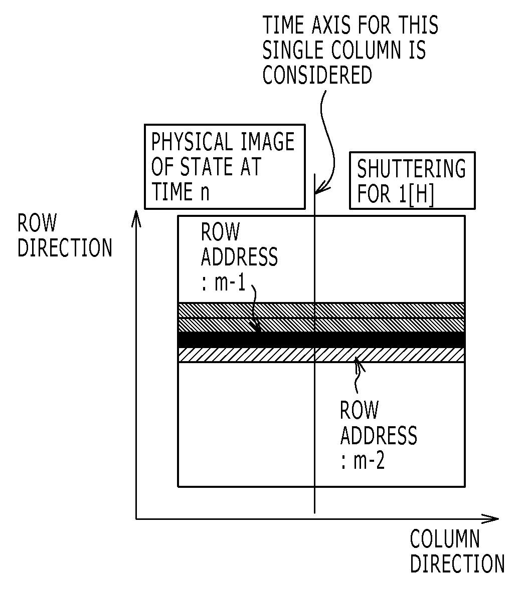
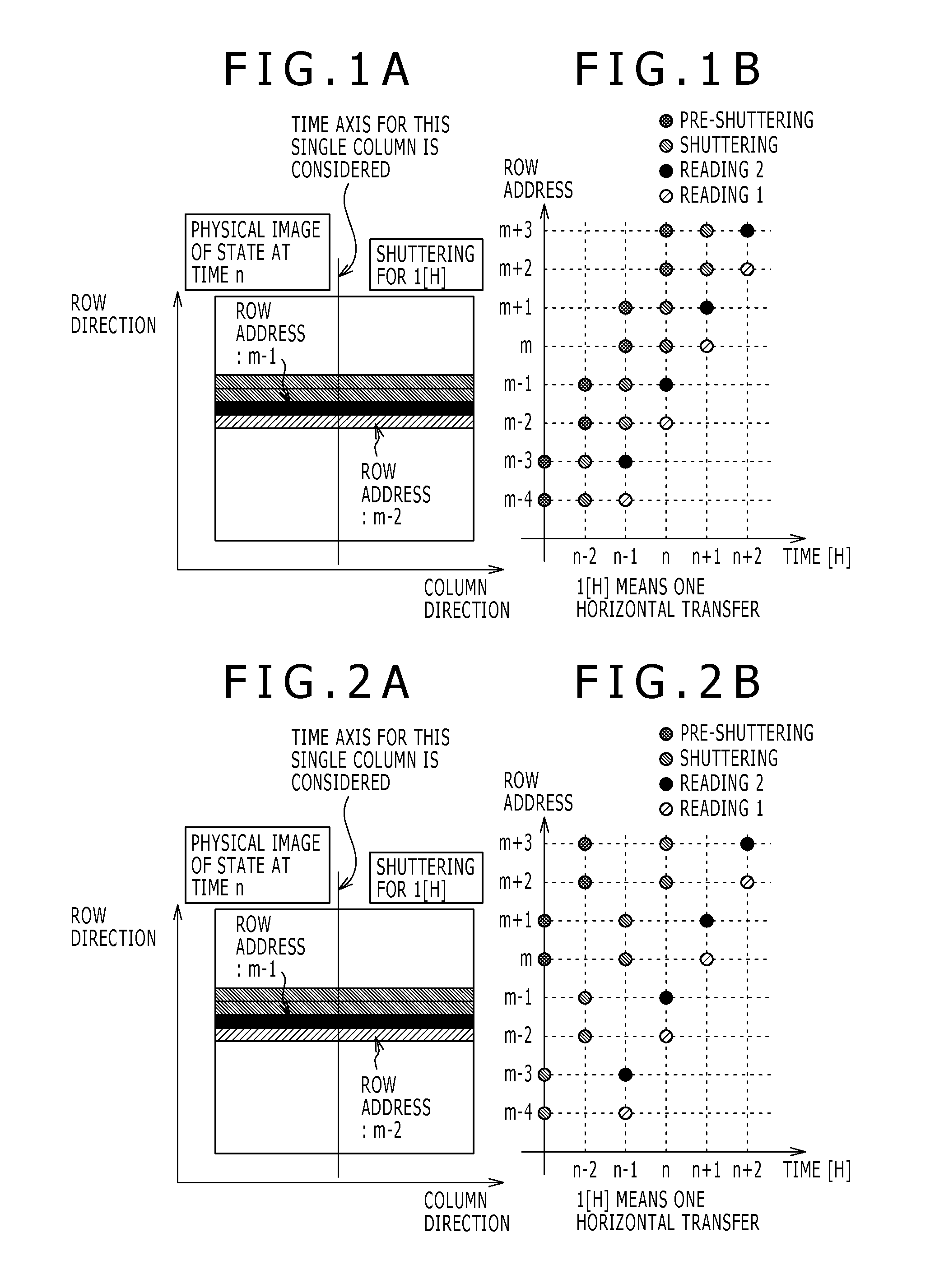
[0037]FIGS. 1A and 1B are diagrams for explaining a first example of the solid-state imaging device according to the embodiment of the present invention, in which FIG. 1B shows shutter operation timings with a horizontal axis indicating a time [H] and a vertical axis indicating a row address, and FIG. 1A represents a state at a time n[H] as a physical image. In the solid-state imaging device according to the first embodiment, a signal charge storing period is set to one horizontal period, and that the solid-state imaging device is of a type which reads two rows simultaneously (a type in which two adjacent rows are set to a single group).

[0038]Here, i...


PUM


Abstract

There is provided a solid-state imaging device having a pixel array section in which pixels including photoelectric conversion elements are arranged in a matrix form, and sweeping out unnecessary charges by setting a predetermined number, two or more, of adjacent rows or a predetermined number, two or more, of adjacent columns, in the pixel array section, to a single group, and by applying a shutter pulse in units of groups before storing signal charges, and sequentially reading the signal charges in the units of groups. In the solid-state imaging device, a pre-shutter pulse is applied to pixels belonging to at least a single row or a single column within a succeeding group and adjacent to a preceding group, prior to the shutter pulse, before a reading timing for the preceding group, to sweep out unnecessary charges stored in the pixels.

Description

BACKGROUND OF THE INVENTION[0001]1. Field of the Invention[0002]The present invention relates to a solid-state imaging device and an image capture apparatus. More particularly, the invention is directed to a solid-state imaging device and an image capture apparatus which, by setting a predetermined number, two or more, of rows or a predetermined number, two or more, of columns to a single group, sequentially read signal charges for each group.[0003]2. Description of Related Art[0004]In X-Y addressable solid-state imaging devices typically represented by CMOS (Complementary Metal Oxide Semiconductor) image sensors, pixels can be selected in units of rows, columns, or pixels, from a pixel array section in which pixels including photoelectric conversion elements are arranged two-dimensionally in a matrix form, so that by specifying an arbitrary area in the pixel array section, pixel information in the arbitrary area can be partially cut out and read. See Japanese Patent Application Pub...

Claims


Application Information

Patent Timeline
Patent Type & Authority Applications(United States)
IPC IPC(8): H04N5/335H04N5/341H04N5/353H04N5/359H04N5/369H04N5/374
CPCH04N3/1568H04N5/3594H04N5/335H04N25/441H04N25/531H04N25/621H04N25/623H04N25/53H04N25/76
Inventor ABIRU, TAKAHIROSUZUKI, RYOJIMAKINO, EIJIUSUI, TAKAYUKI
Owner SONY CORP
Why Eureka
Try Eureka