Imaging device and camera

Inactive Publication Date: 2008-09-04
SONY CORP
View PDF3 Cites 42 Cited by
  • Summary
  • Abstract
  • Description
  • Claims
  • Application Information

AI Technical Summary

Benefits of technology

[0026]According to the embodiments of the invention, the noise level can be reduced

Problems solved by technology

The imaging device of such a configuration, however, often causes a phenomenon of noise streaks of generating streaks (horizontal streaks) in the line direction of a captured image.
The issue here is that if the reference signal includes any noise, the time to be taken until the completion of such a signal comparison process in the voltage comparison sec

Method used


Image

  • Imaging device and camera
  • Imaging device and camera
  • Imaging device and camera

Examples


Example

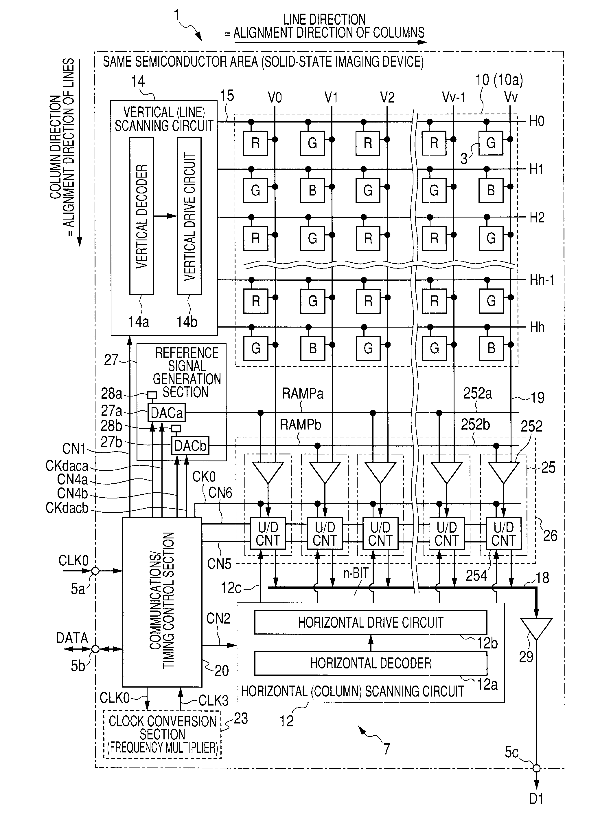
[0039]In the below, an embodiment of the invention is described with reference to the accompanying drawings. Note that, in the below, exemplified is a case where a CMOS imaging device being an exemplary imaging device of X-Y address type is used as a device. In the CMOS imaging device, every pixel is presumed as being an NMOS (N-channel Metal Oxide Semiconductor) or a PMOS (P-channel Metal Oxide Semiconductor).

[0040]This is surely no more than an example, and a target device is not restrictive to an imaging device of MOS (Metal Oxide Semiconductor) type. The following embodiment can be entirely applicable to every type of semiconductor device for use to detect a physical quantity distribution including a plurality of lines or matrixes of unit components being sensitive to electromagnetic waves coming from the outside, e.g., lights and radiation rays.

[0041]FIG. 1 is a diagram schematically showing the configuration of an exemplary CMOS imaging device, i.e., COMS image sensor, as an e...


PUM


Abstract

An imaging device is disclosed. The device includes: a unit pixel that outputs an analog electric signal in accordance with a signal charge; a local voltage supply circuit that generates a local voltage different from an operation voltage; a reference signal generation section that generates a reference signal based on the local voltage provided by the local voltage supply circuit; and a processing section that converts, by referring to the reference signal generated by the reference signal generation section, the analog signal provided by the unit pixel into a digital signal. In the imaging device, the reference signal generation section keeps constant a load current of the local voltage supply circuit in an operating state.

Description

CROSS REFERENCES TO RELATED APPLICATIONS[0001]The present invention contains subject matter related to Japanese Patent Application JP 2007-051303 filed in the Japanese Patent Office on Mar. 1, 2007, the entire contents of which being incorporated herein by reference.BACKGROUND OF THE INVENTION[0002]1. Field of the Invention[0003]The present invention relates to an imaging device utilizing a CMOS (Complementary Metal Oxide Semiconductor) sensor or others, and a camera.[0004]2. Description Of the Related Art[0005]As an example, a CMOS imaging device of Patent Document 1 (JP-A-2005-328135) converts, by pixels, any imaged object into an electric signal (pixel signal), and converts the analog electric signal into digital image data using an analog digital converter equipped in a column processing circuit.[0006]By taking as an example the column processing circuit of the CMOS imaging device of Patent Document 1, the outline of the operation thereof is described by referring to FIG. 12.[00...

Claims


Application Information

Patent Timeline
IPC IPC(8): H04N5/335H01L27/146H04N5/357H04N5/369H04N5/374H04N5/378
CPCH04N5/3658H04N5/3655H04N25/673H04N25/677
Inventor WAKABAYASHI, HAYATOINADA, YOSHIAKI
Owner SONY CORP
Why Eureka
Try Eureka