
Contact insert for a microcircuit test socket

Active Publication Date: 2008-09-11
JOHNSTECH INT
View PDF9 Cites 6 Cited by
  • Summary
  • Abstract
  • Description
  • Claims
  • Application Information

AI Technical Summary

Benefits of technology

[0025]This design lends itself to a further improvement that provides biasing force that presses the load board CG contact end firmly against the load board and the load board ground terminal to limit migration of debris into the interface between the insert and the load board ground terminal.

Problems solved by technology

The manufacturing processes for microcircuits cannot guarantee that every microcircuit is fully functional.
Dimensions of individual microcircuits are microscopic and process steps very complex, so small or subtle failures in a manufacturing process can often result in defective devices.
While the cost of a microcircuit is frequently quite small, mounting one on a circuit board adds substantial value due to the cost of the circuit board and the manufacturing cost itself.
Once mounted on a circuit board, removing a microcircuit often ruins the circuit board.
Thus, if the microcircuit is defective, the circuit board itself is probably ruined as well, meaning that the entire value of the circuit board at that point is lost.
Each microcircuit must be tested in a way that identifies nearly all defective devices, but only rarely identifies good devices as defective.
Either kind of error adds cost to the overall manufacturing process.
Microcircuit test equipment itself is quite complex.
Because of the small size of microcircuit terminals and the small spacing between adjacent pairs, even small alignment errors between the test equipment contacts and microcircuit terminal pads will result in incorrect connections.
Connections to the microcircuit that are misaligned or otherwise incorrect will cause the test equipment to identify the microcircuit, that is, the device under test (DUT), as defective, even though the reason for the failure is the defective connections rather than defects in the DUT itself.
A further problem in microcircuit test equipment arises in automated testing, where a single system may test 100 or more DUTs a minute.
The sheer number of tests can cause wear on the test equipment contacts as the DUT terminals mate with the test equipment contacts and wipe against them.
The particles and other contaminants may eventually build to a point where they interfere with the electrical connections between the DUT terminals and the test equipment contacts during testing, which may result in false indications that the DUT is defective.
The particles may also create leakage paths between adjacent test equipment contacts, also leading to false indications that the DUT is defective.
The effect of this wear is to require replacement of these components, during which time the test equipment cannot be used.
The wear also creates debris that as explained above, may interfere with the testing process.

Method used


Image

  • Contact insert for a microcircuit test socket
  • Contact insert for a microcircuit test socket
  • Contact insert for a microcircuit test socket

Examples


Embodiment Construction

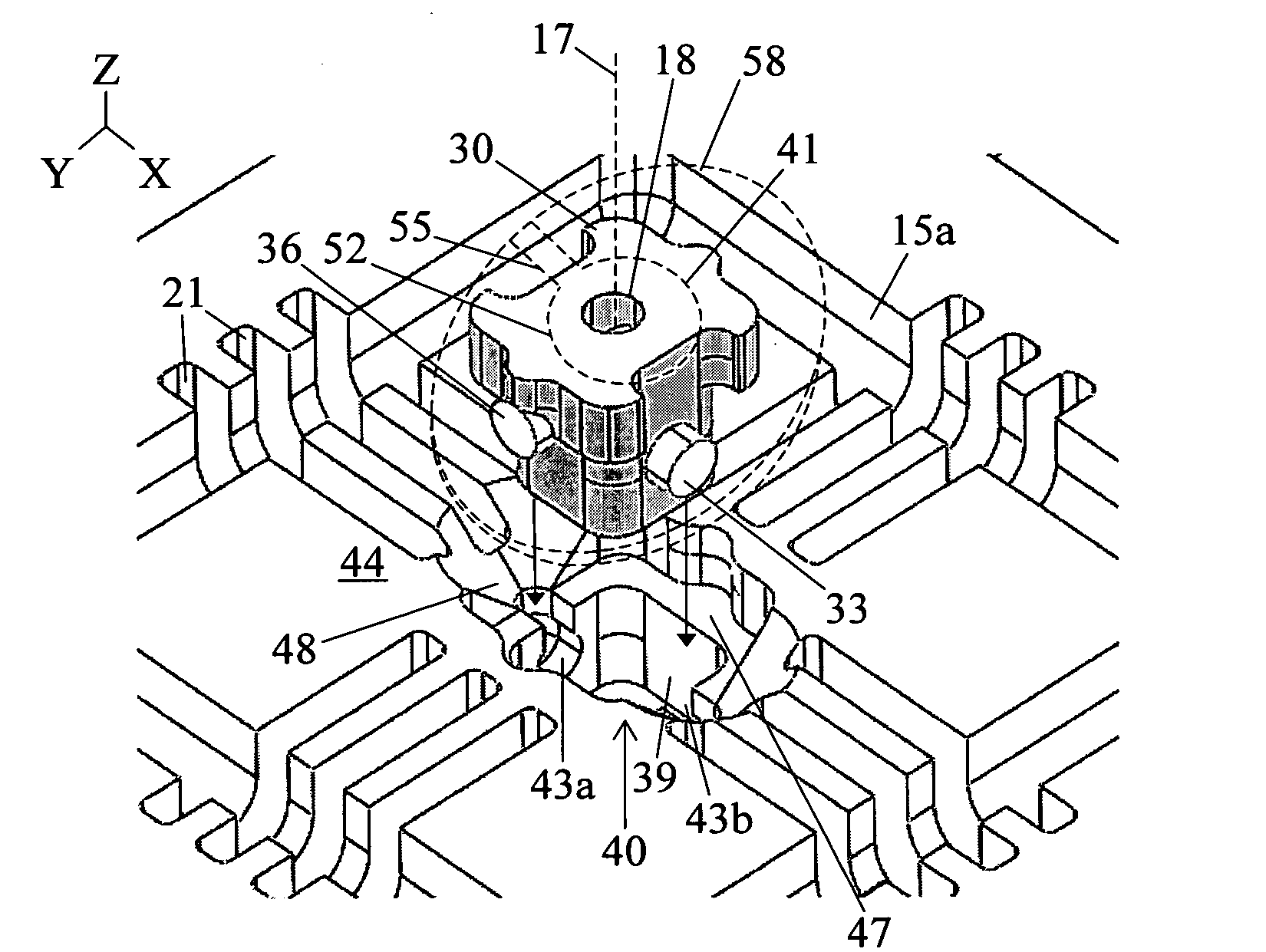
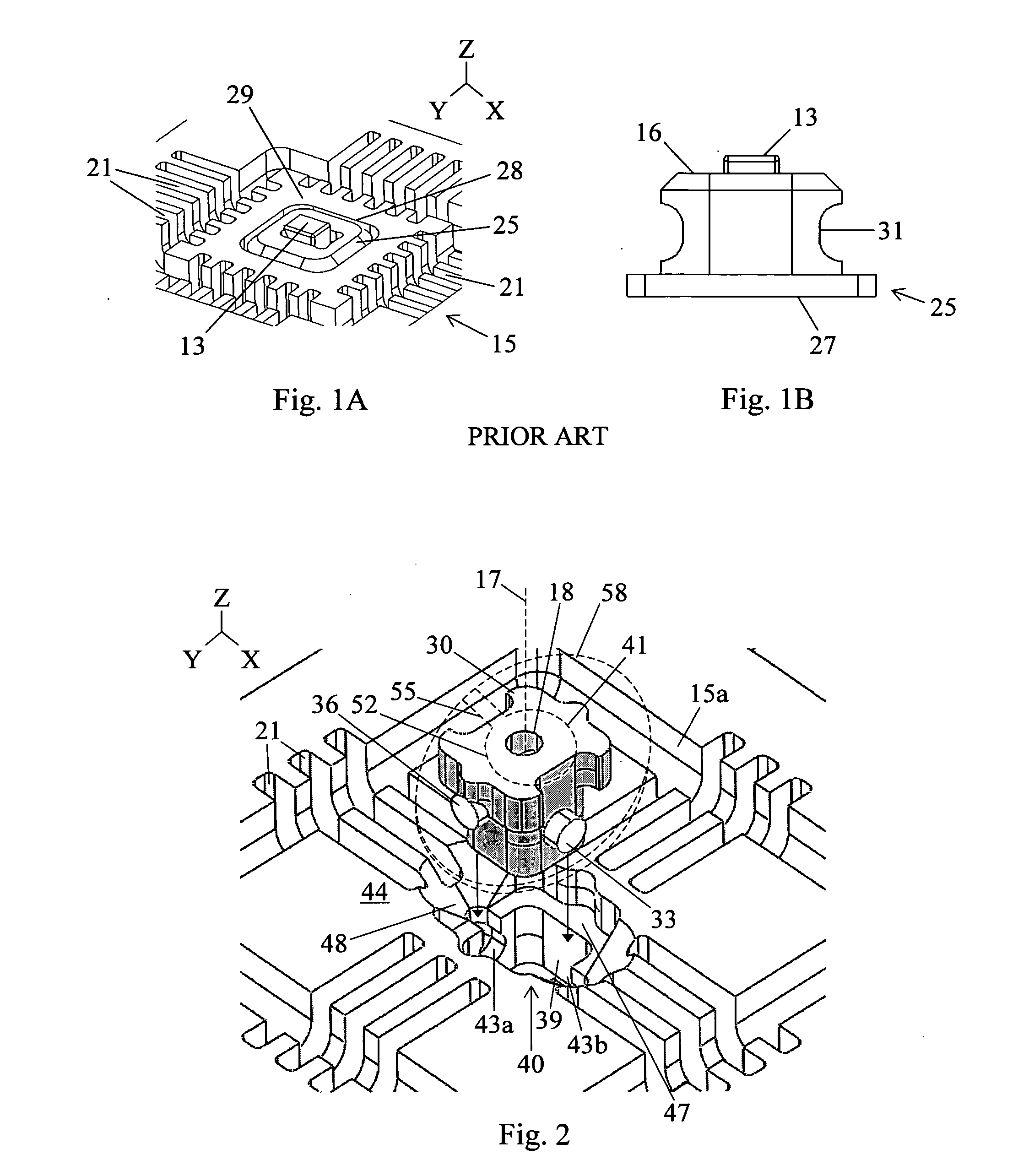
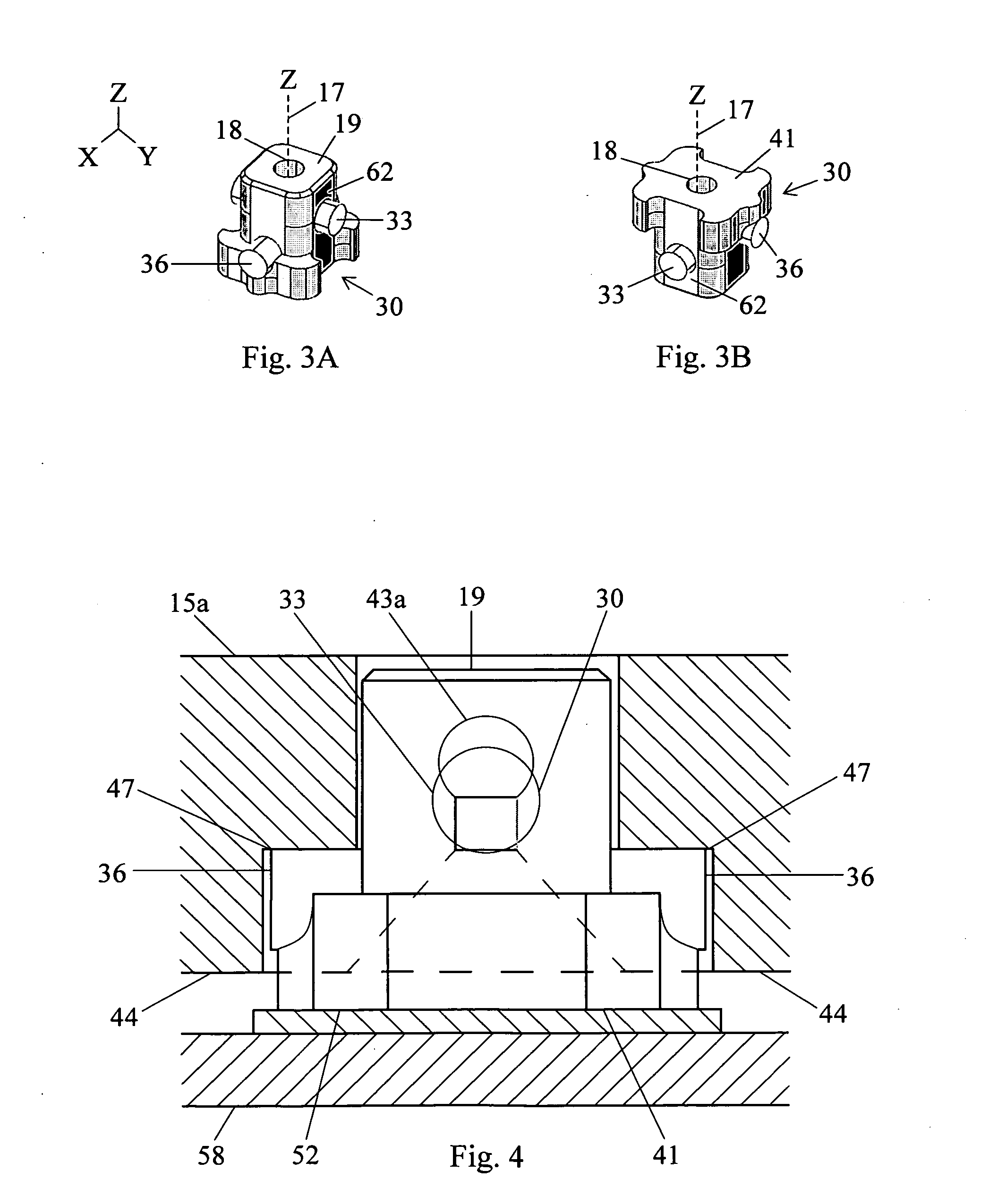
[0031]The FIG. 2 perspective view shows a modified housing 15a from the load board side, i.e. bottom facing up, with an insert 30 aligned for inserting in an aperture 40 in housing 15a. Walls 39 define aperture 40 and are substantially parallel with a Z axis 17 of aperture 40.

[0032]Portions of housing 15a surrounding aperture 40 have slots 21 for retaining and aligning test contacts (not shown) that make electrical contact with the S & P terminals of the DUT. Aperture 40 passes completely through housing 15a from surface 44 on the load board side to the DUT mounting side. Housing 15a has a bevel 48 surrounding aperture 40 that facilitates the process of installing an insert 30 into aperture 40. Surface 44 is substantially coplanar with the upwardly-facing surfaces between individual slots 21.

[0033]FIG. 2 shows a portion of a load board 58 in phantom with a first side facing insert 30 (and facing away from the viewer as shown in FIG. 2). The load board 58 first side is flat and when ...


PUM


Abstract

A system for testing a microcircuit having a center ground (CG) terminal has an insert for electrically connecting the CG terminal to a ground contact on a load board. The insert is held within a housing by compression and frictional interaction between a resilient projection carried by the insert and a slot in a wall of an aperture holding the insert.

Description

CROSS-REFERENCE TO RELATED APPLICATIONS[0001]This is a regular application filed under 35 U.S.C. § 111(a) claiming priority, under 35 U.S.C. § 119(e)(1), of provisional application Ser. No. 60 / 887,983, previously filed Feb. 2, 2007 under 35 U.S.C. § 111(b).BACKGROUND OF THE INVENTION[0002]The invention pertains to improvements to equipment for testing microcircuits. The manufacturing processes for microcircuits cannot guarantee that every microcircuit is fully functional. Dimensions of individual microcircuits are microscopic and process steps very complex, so small or subtle failures in a manufacturing process can often result in defective devices. For this reason, microcircuit testing has become widely practiced, in both the semiconductor manufacturing and the circuit board assembly industries.[0003]While the cost of a microcircuit is frequently quite small, mounting one on a circuit board adds substantial value due to the cost of the circuit board and the manufacturing cost itsel...

Claims


Application Information

Patent Timeline
IPC IPC(8): G01R1/02
CPCG01R1/0466
Inventor ALLADIO, PATRICK J.WARWICK, BRIAN K.
Owner JOHNSTECH INT
Learn More