

Power Supply Device
a power supply device and switching element technology, applied in the direction of dc-ac conversion without reversal, process and machine control, instruments, etc., can solve the problem that the power supply device has a small switching loss in the switching elements, and achieve the effect of small switching loss
- Summary
- Abstract
- Description
- Claims
- Application Information
AI Technical Summary
Benefits of technology
Problems solved by technology
Method used
Image

Examples
exemplary embodiment 1
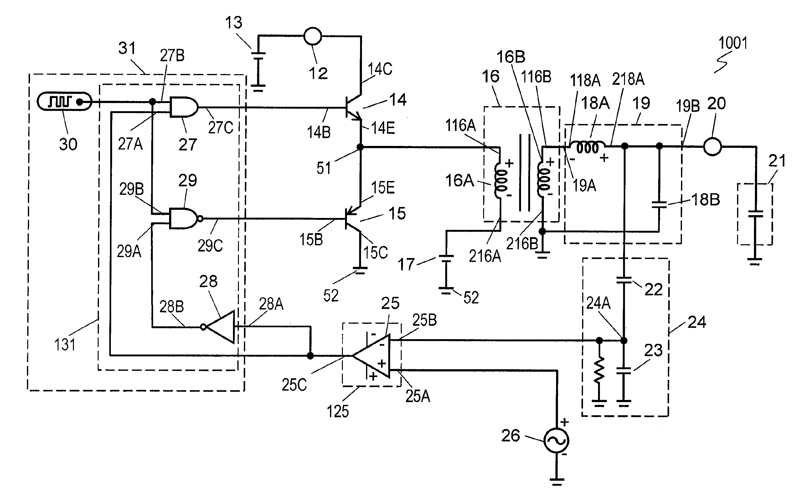
[0035]FIG. 1A is a circuit diagram of power supply device 1001 in accordance with Exemplary Embodiment 1 of the present invention. Input terminal 12 is arranged to be connected to direct-current (DC) power supply 13. Collector 14C of NPN transistor 14, a switching element capable of conducting and nonconducting, is connected to input terminal 12. Emitter 15E of PNP transistor 15, a switching element capable of conducting and nonconducting, is connected to emitter 14E of transistor 14 at node 51. Collector 15C of transistor 15 is connected to ground 52. Positive end 116A of primary coil 16A of transformer 16 is connected to node 51. Power supply 17 for setting an operating point is connected to negative end 216A of primary coil 16A. Power supply 17 fixes an electric potential at positive end 216A of primary coil 16A of transformer 16 to a potential between an electric potential at input terminal 12 and ground 52, for example, to a half the electric potential at input terminal 12. Inp...
exemplary embodiment 2
[0054]FIG. 3 is a circuit diagram of power supply device 1002 in accordance with Exemplary Embodiment 2 of the present invention. In FIG. 3, the components identical to those of power supply device 1001 according to Embodiment 1 shown in FIG. 1 are denoted by the same reference numerals, and their description will be omitted.
[0055]Power supply device 1002 show in FIG. 3 includes N-channel field-effect transistors (FETs) 40 and 41 as switching elements instead of transistors 14 and 15 of power supply device 1001 shown in FIG. 1. A gate, drain, and source of FET 40 are connected positions connected to base 14B, collector 14C, and emitter 14E of transistor 14 of power supply device 1001 of FIG. 1, respectively. A gate, drain, and source of FET 41 are connected to positions connected to base 15B, collector 15C, and emitter 15E of transistor 15 of power supply device 1001 of FIG. 1, respectively. In other words, the source of FET 40 and the drain of FET41 are connected to each other at n...
exemplary embodiment 3
[0059]FIG. 4 is a circuit diagram of power supply device 1003 in accordance with Exemplary Embodiment 3 of the present invention. In FIG. 4 components identical to those of power supply device 1002 of Embodiment 2 shown in FIG. 3 are denoted by the same reference numerals, and their description will be omitted.
[0060]Power supply device 1003 includes field-effect transistors (FETs) 35 and 36 and transformer 34 instead of FETs 40 and 41 and transformer 16 of power supply device 1002 shown in FIG. 3. Transformer 34 includes two primary coils 34A and 34B and secondary coil 34C. Positive end 134A of primary coil 34A and negative end 234B of primary coil 34B are connected to input terminal 12 arranged to be connected to direct-current (DC) power supply 13. Negative end 234A of primary coil 34A is connected to drain 35D of FET 35. Positive end 134B of primary coil 34B is connected to drain 36D of FET 36. Similar to positive end 116B and negative end 216B of secondary coil 16B of transforme...
PUM
 Abstract
Description
Claims
Application Information