
Fabrication method of size-controlled, spatially distributed nanostructures by atomic layer deposition

Inactive Publication Date: 2008-11-06
HONDA MOTOR CO LTD +1
View PDF6 Cites 41 Cited by
  • Summary
  • Abstract
  • Description
  • Claims
  • Application Information

AI Technical Summary

Benefits of technology

[0019]Some key advantages of the current invention include use of vapor phase method for synthesis of nanoparticles and other nanoscale objects with control over size and average spacing. These aspects eliminate the need for a surface capping layer or other stabilization layer on the nanoparticles. The method can be used on highly porous substrates. The ALD-based method allows size and dispersion-controlled nanoparticles to be controllably deposited in complex, porous or highly structured substrates. Catalyst geometry is enhanced by controlling the porosity of the material or the feature size of the film's mesh structure, for catalytic applications. A reduced catalyst loading is provided by controlling the size and distribution of the catalyst. Material selection can be broad, since ALD can be used to deposit range of materials, including conductors, semiconductors, insulators, catalysts and photo-catalysts, and the choice of substrate material is also broad.

Problems solved by technology

All of the aforementioned techniques have lacked control of the size and spacing of the desired nanoparticles.

Method used


Image

  • Fabrication method of size-controlled, spatially distributed nanostructures by atomic layer deposition
  • Fabrication method of size-controlled, spatially distributed nanostructures by atomic layer deposition
  • Fabrication method of size-controlled, spatially distributed nanostructures by atomic layer deposition

Examples


Embodiment Construction

[0034]Although the following detailed description contains many specifics for the purposes of illustration, anyone of ordinary skill in the art will readily appreciate that many variations and alterations to the following exemplary details are within the scope of the invention. Accordingly, the following preferred embodiment of the invention is set forth without any loss of generality to, and without imposing limitations upon, the claimed invention.

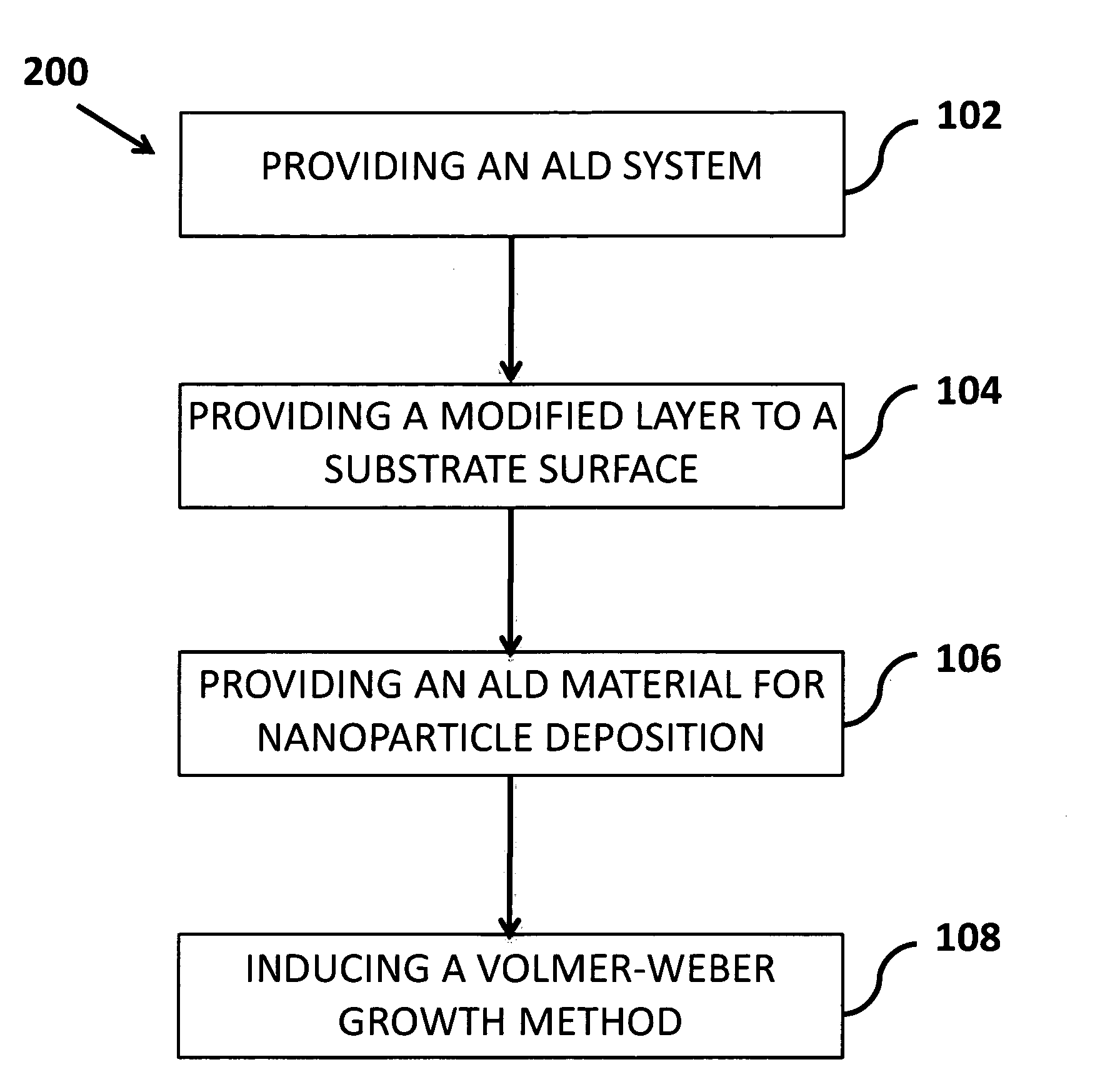
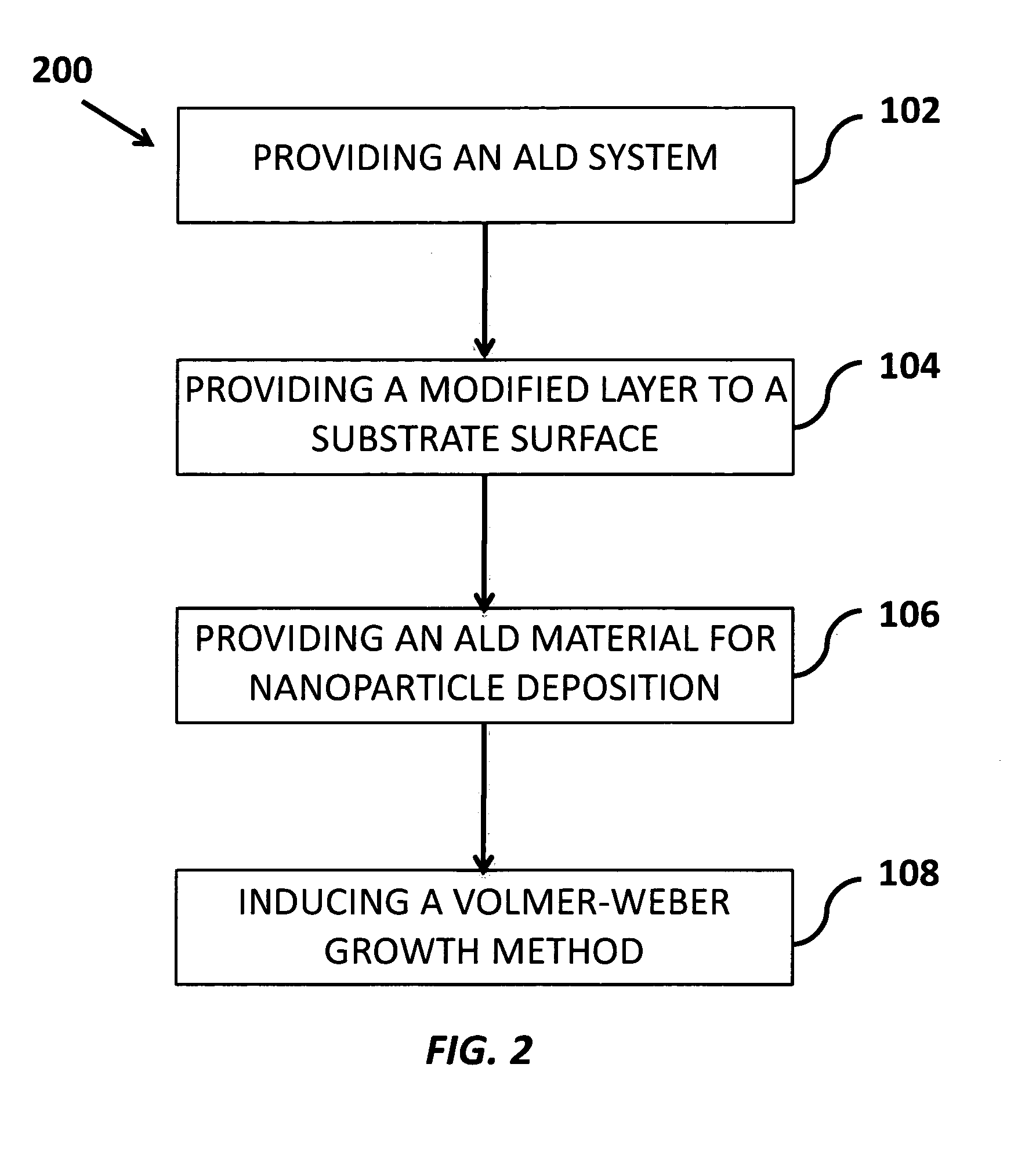
[0035]FIG. 2 is a flow diagram showing the steps of the method for growing nanoparticles 200 on both flat and highly structured surfaces in which the size and average spacing of the nanoparticles can be controlled, according to the current invention. The method 200 includes using an atomic layer deposition (ALD) system 202, providing a modified layer to the substrate surface 204 and providing an ALD material for nanoparticle deposition 206. The method induces a Volmer-Weber growth method 208, where islands of the nanoparticles are formed ...


PUM

PropertyMeasurementUnit
Timeaaaaaaaaaa
Timeaaaaaaaaaa
Water contact angleaaaaaaaaaa

Abstract

A method of growing spatially-separated and size-controlled particles on substrate surfaces is provided. The method utilizes chemical modification of the substrate surface, an atomic layer deposition (ALD) system, providing a modified layer to the substrate surface and providing an ALD material for nanoparticle deposition. The method induces a Volmer-Weber growth method, where islands of the nanoparticles are formed on the surface. The modified layer controls a number of nucleation sites on the surface, where controlling the number of ALD cycles limits an amount of deposited the material for discrete the nanoparticles. The modified layer can include self-assembled monolayers, modified hydrophobicity of the surface, H-terminated surfaces, and varying functional groups within the modified layer, where thermally attached alkenes, photochemically attached alkenes, thermally attached alkynes or photochemically attached alkynes are attached to the H-terminated surfaces, and the density of the nucleation sites of the nanoparticles are thereby managed.

Description

CROSS-REFERENCE TO RELATED APPLICATIONS[0001]This application is cross-referenced to and claims the benefit from U.S. Provisional Patent Application 60 / 901,584 filed Feb. 14, 2007, which is hereby incorporated by reference.FIELD OF THE INVENTION[0002]The invention relates generally to fabrication methods of nanostructures, including nanoparticles, nanodots, nanowires and nanorods. More particularly, the invention relates to fabrication methods with controllable size and spacing on a variety of substrates and substrate geometries using atomic layer deposition.BACKGROUND[0003]Atomic layer deposition (ALD) is a process for depositing highly uniform and conformal thin films by alternating exposures of a surface to vapors of two chemical reactants. For example, it is useful for depositing high-permittivity metal oxide dielectrics such as ZrO2 or HfO2 to replace SiO2 in future generation metal-oxide-silicon (MOS) transistors. Other applications include luminescent materials for photonics,...

Claims


Application Information

Patent Timeline
IPC IPC(8): C23C16/00
CPCC23C16/04C23C16/45525
Inventor BENT, STACEY F.CHEN, RONGJIANG, XIRONGMULLINGS, MARJA N.SAITO, YUJI
Owner HONDA MOTOR CO LTD
Learn More