Memory Device with Error Correction Capability and Preemptive Partial Word Write Operation

a memory device and partial word technology, applied in error detection/correction, digital storage, instruments, etc., can solve the problems of reducing the yield of the integrated circuit manufacturing process, reducing the time required for most partial word write operations, and causing the error of memory cells to be read with incorrect data

Active Publication Date: 2008-12-04
AVAGO TECH INT SALES PTE LTD
View PDF2 Cites 15 Cited by
  • Summary
  • Abstract
  • Description
  • Claims
  • Application Information

AI Technical Summary

Benefits of technology

[0017]Advantageously, the preemptive partial word write approach removes the ECC decode process and its associated correct process from the critical timing path of the partial word write operation. The time required to perform a partial word write operation is thus typically reduced by the time ...

Problems solved by technology

Semiconductor memory devices are subject to defects that may cause some memory cells to be read with incorrect data.
Such defects are generally discovered during post-manufacture testing of integrated circuit memory devices.
Defective memory devices may need to be discarded, thereby reducing the yield of the integrated circuit manufacturing process, and increasing the net manufacturing costs for the non-defective devices.
Requiring two clock cycles is disadvantageous because it slows down the data transfer rate between the memory device and a higher-level system...

Method used


Image

  • Memory Device with Error Correction Capability and Preemptive Partial Word Write Operation
  • Memory Device with Error Correction Capability and Preemptive Partial Word Write Operation
  • Memory Device with Error Correction Capability and Preemptive Partial Word Write Operation

Examples


Embodiment Construction

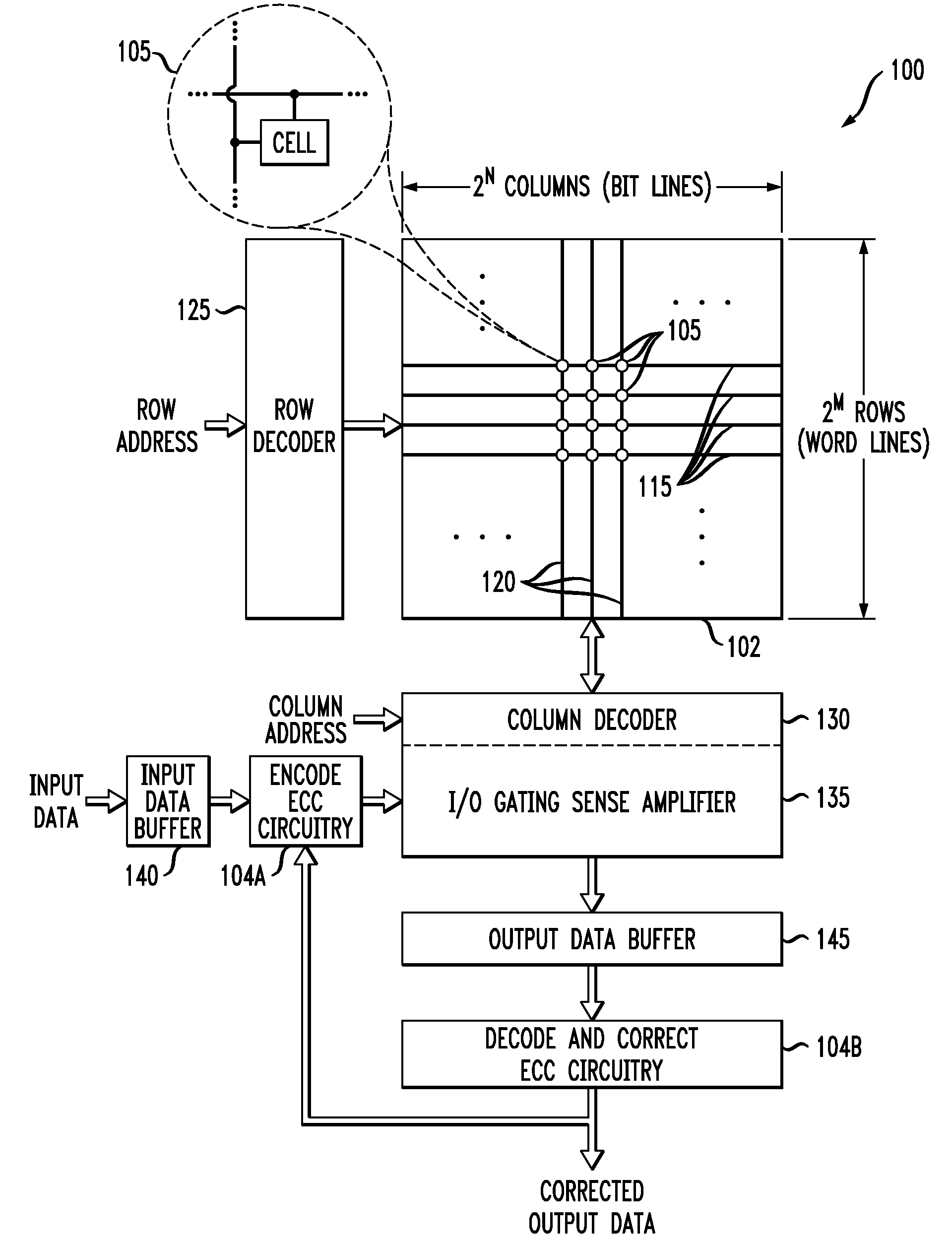
[0021]The invention will be illustrated herein in conjunction with exemplary semiconductor memory devices and associated error correction circuitry. It should be understood, however, that the invention is more generally applicable to any semiconductor memory device, and may be implemented using error correction circuitry other than that specifically shown in conjunction with the illustrative embodiments.

[0022]The present invention may be implemented in memory devices of the type described in PCT International Application No. PCT / US07 / 67502, filed Apr. 26, 2007 and entitled “Memory Device with Error Correction Capability and Efficient Partial Word Write Operation,” which is commonly assigned herewith and incorporated by reference herein. However, such devices are not required for implementation of the present invention.

[0023]FIG. 1 shows a simplified diagram of a memory device 100 in accordance with an illustrative embodiment of the invention. The memory device 100 comprises a memory...


PUM


Abstract

A memory device comprises a memory array and error correction circuitry coupled to the memory array. The memory device is configured to perform a partial word write operation in which an error correction code encode process for the given retrieved word is initiated prior to completion of an error correction code decode process for the given retrieved word based on an assumption that the error correction code decode process will not indicate an error in the given retrieved word. If the error correction code decode process when completed indicates an error in the given retrieved word, the error in the given retrieved word is corrected in the error correction circuitry, and the error correction code encode process is restarted using the corrected word. The error correction code decode process and an associated correct process are thereby removed from a critical timing path of the partial word write operation.

Description

FIELD OF THE INVENTION[0001]The present invention relates generally to semiconductor memory devices, and more particularly to memory devices which incorporate error correction capability.BACKGROUND OF THE INVENTION[0002]Semiconductor memory devices are subject to defects that may cause some memory cells to be read with incorrect data. Such defects are generally discovered during post-manufacture testing of integrated circuit memory devices. Defective memory devices may need to be discarded, thereby reducing the yield of the integrated circuit manufacturing process, and increasing the net manufacturing costs for the non-defective devices.[0003]A number of techniques are known for configuring a memory device to remain operative in the presence of defects. One such technique involves incorporating redundant lines, rows or blocks of cells into the device. This allows lines, rows or blocks having defective cells to be replaced with corresponding non-defective redundant elements. Volatile...

Claims


Application Information

Patent Timeline
IPC IPC(8): G11C29/00
CPCG06F11/1044G11C7/1006G11C2029/0411
Inventor KOHLER, ROSS A.MCPARTLAND, RICHARD J.WERNER, WAYNE E.
Owner AVAGO TECH INT SALES PTE LTD
Why Eureka
Try Eureka