Low area screen printed metal contact structure and method

Inactive Publication Date: 2009-01-08
NEWSOUTH INNOVATIONS PTY LTD +1
View PDF5 Cites 52 Cited by
  • Summary
  • Abstract
  • Description
  • Claims
  • Application Information

AI Technical Summary

Benefits of technology

[0026]To simplify the doping of the walls of the depressions (wells or grooves) in commercial processes, by reducing the number of processing steps, and thereby reducing the cost, it is possible to deliberately add dopants into the surface dielectric layer such that when the laser is used to drill surface depressions for the contacts some of the

Problems solved by technology

Secondly, it is used to passivate the top surface of the silicon wafer.
Deposition by plasma enhanced chemical vapour deposition (PECVD) also provides thinner deposited layers within grooves and wells due to the restricted access into such regions for the ionic species generated in the plasma and the relatively large surface areas to be coated in such regions.
An important issue when establishing metal contacts to semiconductor material, such as in a solar cell, is the contact resistance between the metal and semiconductor.
This will however increase the dark saturation current for the device due to the increased volume of heavily doped silicon.
A challenge though with using wells or grooves fully covered by the screen-printed metal is that air is trapped in the well or groove.
Thi

Method used


Image

  • Low area screen printed metal contact structure and method
  • Low area screen printed metal contact structure and method
  • Low area screen printed metal contact structure and method

Examples


Example

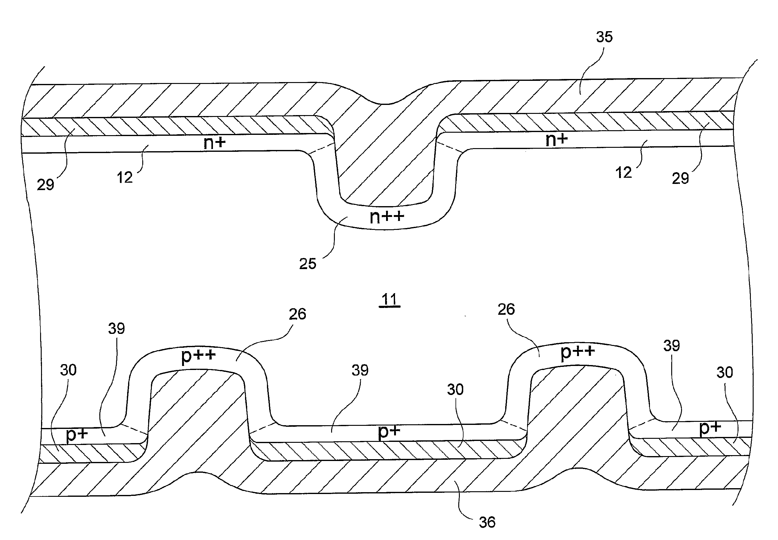
[0045]Referring to the drawings, in embodiments of the present contact structure, a dielectric layer is used across the top surface of a solar cell for four (4) purposes. Firstly, it is used to isolate the subsequently printed screen printed metal from the top surface of the wafer. Secondly, it is used to passivate the top surface of the silicon wafer. Thirdly, it is used as an antireflection coating for the silicon wafer (although this aspect is less important if this metal contacting scheme is being used on the rear surface of a solar cell). Fourthly it is used to provide a reduced thickness (even zero thickness in some cases) layer in regions below the top surface, such as where wells or grooves have been made in the silicon surface prior to depositing the dielectric layer. The purpose of these reduced thickness regions is so that the screen-printed metal is able to be driven through the thinner dielectric layer in these regions so as to contact the underlying silicon, while rema...


PUM


Abstract

A solar cell comprises adjacent regions of oppositely doped semiconductor material forming a pn junction substantially parallel to front and rear surfaces of the solar cell. A surface of the semiconductor material has a plurality of depressions, with semiconductor material regions forming internal wall surface regions of the depressions being doped to the polarity of one of the semiconductor regions, with which they are in electrical communication. The wall surface regions of the depressions are isolated from the other oppositely doped semiconductor region and form contact points for a contact structure contacting the surface in which the depressions are formed. A dielectric layer is formed over the surface, the dielectric layer being thinner or non-existent in at least a portion of each depression, such that a screen printed metal contact structure formed over the dielectric layer and extending into the depressions makes contact with the semiconductor material in the depressions after sintering.

Description

[0001]The present invention relates to the field of photovoltaics and in particular provides a new contact structure for commercially produced solar cells.BACKGROUND TO THE INVENTION [0002]High performance solar cells in general require low area contacts to minimise the contribution of the high recombination velocity metal / silicon interface to the device dark saturation current. Most laboratory solar cells use photolithographic techniques or laser scribing to facilitate the formation of low area metal contacts to the silicon that typically cover less than 1% of the solar cell surface. This minimises the device dark saturation current which in turn maximises the cell open circuit voltage (Voc). The highest Voc values ever achieved for silicon solar cells is in the vicinity of 720 mV, through careful attention to minimising the recombination taking place at the front and rear surfaces and particularly at the metal / silicon interfaces.[0003]In comparison, the dominant commercial solar c...

Claims


Application Information

Patent Timeline
IPC IPC(8): H01L31/00H01L21/22H01L21/00
CPCH01L21/743Y02E10/50H01L31/022433H01L31/022425H01L31/04H01L31/18H01L21/44
Inventor WENHAM, STUART ROSSMAI, LYSHI, ZHENGRONGJI, JINGLIA
Owner NEWSOUTH INNOVATIONS PTY LTD
Why Eureka
Try Eureka