Plasma display panel apparatus and method for driving the same

Inactive Publication Date: 2009-01-15
PANASONIC CORP
View PDF12 Cites 15 Cited by
  • Summary
  • Abstract
  • Description
  • Claims
  • Application Information

AI Technical Summary

Benefits of technology

[0019]The present invention is made in view of the above problems and aims to provide a plasma display panel and a method for driving the plasma display panel capable of image display with no flickering and good quality. These advantageous effects are achieved even if the plasma display panel is in compliance with the high-definition standard and without applying an auxiliary erase pulse after the erase period. More specifically, the advantageous effects are achieved by suppressing problems caused by an erroneous sustain discharge resulting from a strong discharge that may accidentally occur in the reset period.
[0020]In order to solve the above-noted problems associated with the prior art, the present invention provides a method for driving a plasma display apparatus through a driving process according to which each of a plurality of fields includes a plurality of sub-fields. The plasma display apparatus has: display electrode pairs each composed of a scan electrode and a sustain electrode; a plurality of address electrodes that are separated from the display electrode pairs by a discharge space and that extend in a direction intersecting the display electrode pairs; and a plurality of discharge cells formed at locations corresponding to the intersections. According to the method, at least one sub-field in each field includes an all-cell reset period in which an erase discharge is caused in all the discharge cells. The all-cell reset period includes: a first step of applying an ascending ramp waveform voltage to the scan electrodes, so that a first reset discharge is caused between each of the scan electrodes and a corresponding one of the data and / or sustain electrodes; a second step of applying a descending ramp waveform voltage to the scan electrodes, so that a second reset discharge is caused between each of the scan electrodes and a corresponding one of the data and / or sustain electrodes; and an excessive wall voltage erase step of applying, after the first step ends, a potential-change waveform to at least either the scan electrodes, the sustain electrodes, or the address electrodes, so that an excessive wall voltage in each discharge cell is erased, the potential-change waveform having a ramp that is steeper than the descending ramp of the waveform voltage applied in the second step to the scan electrodes.
[0021]The potential-change waveform may be a pulsed waveform. Further, the potential-change may be applied to the scan electrodes. Further, a potential of the sustain electrodes may be made to change during or after application of the potential-change waveform to the scan electrodes.
[0022]Alternatively, the potential-change waveform may be applied to the sustain electrodes. In this case, the potential-change waveform may be applied to the sustain electrodes after the first step ends and before a potential of the scan electrodes changes. Alternatively, the potential-change waveform may be applied to the sustain electrodes after the first step ends and after a potential of the scan electrodes changes.
[0023]Alternatively, the potential-change waveform may be applied to the address electrodes. In this case, the address electrodes may act as positively charged electrodes during the potential-change waveform application.
[0024]The potential-change waveform may be applied to the address electrodes either before or after a potential of the sustain electrodes changes.

Problems solved by technology

Unfortunately, however, the increase in Xe partial pressure involves a longer discharge delay.
This discharge delay is problematic especially when there is an insufficient amount of priming (an initiator of discharge=excited particles).
As a result, it is no longer possible to properly control a sustain discharge, which leads to image deterioration.
In addition, such an abnormal reset emission may be caused due to the factors other than the partial pressure of Xenon.

Method used


Image

  • Plasma display panel apparatus and method for driving the same
  • Plasma display panel apparatus and method for driving the same
  • Plasma display panel apparatus and method for driving the same

Examples


embodiment 1

(Overall Structure of PDP Apparatus)

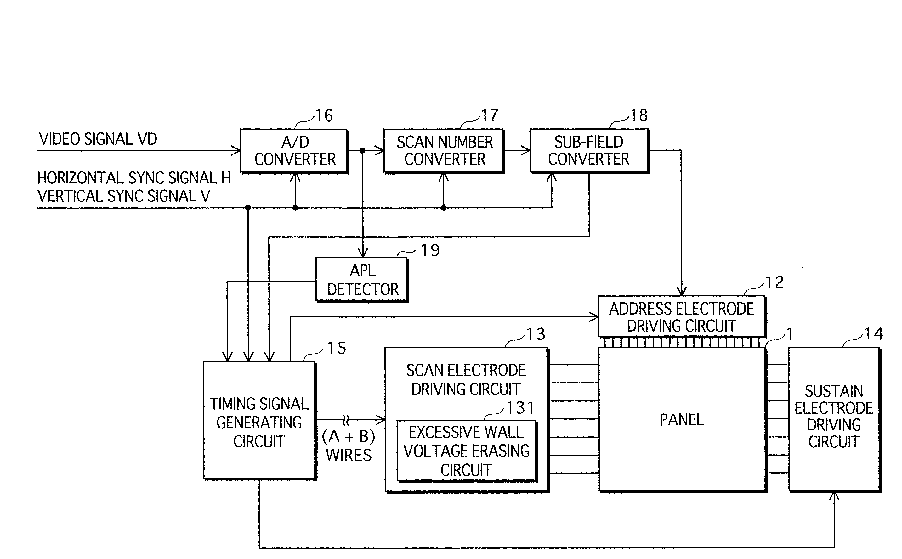
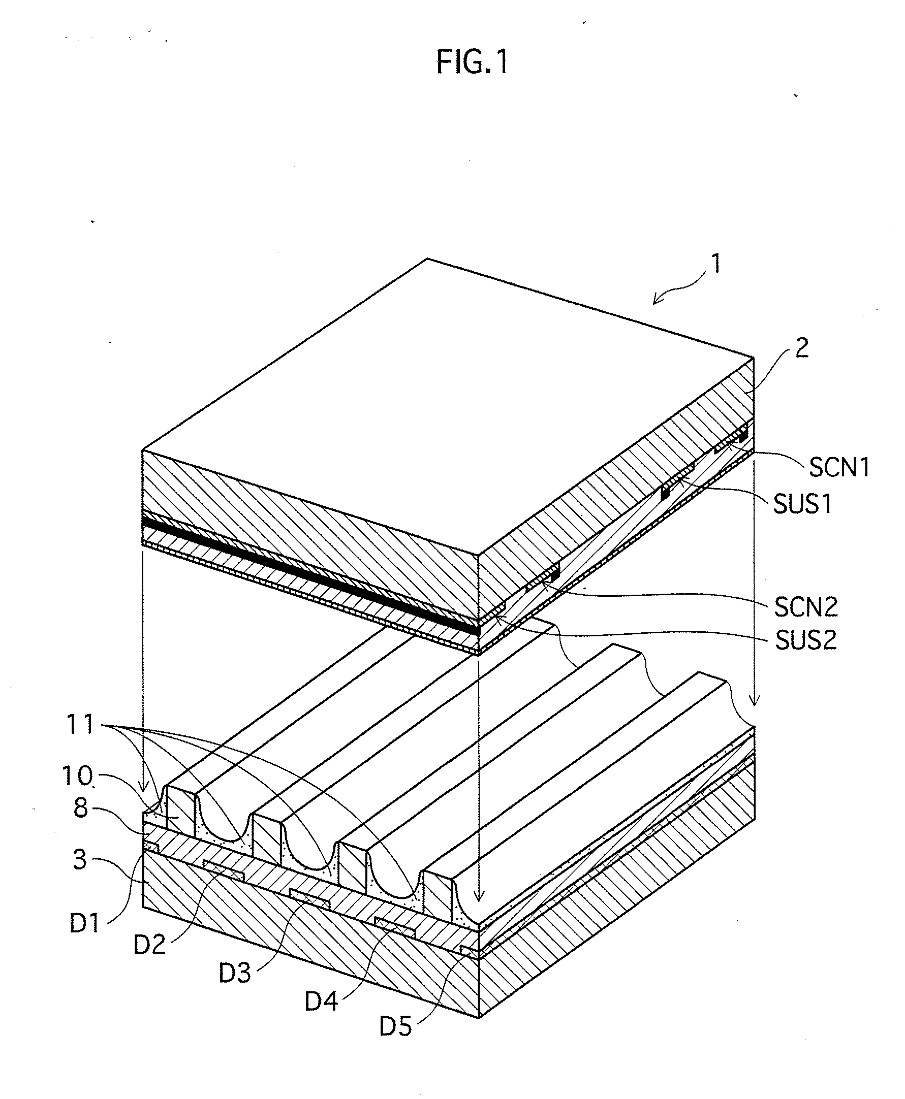
[0070]FIG. 1 is a partial oblique view of an exemplary PDP structure. A PDP 1 illustrated in the figure is generally identical to the conventional structure described above. Thus, overlapping descriptions will be omitted. It should be noted, in addition, that the PDP and the drive device of the substantially same structures are employed throughout all the embodiments below.

[0071]The PDP 1 includes a front substrate (front panel) 2 and a back substrate (back panel) 3 and a main part of each substrate is constituted of a grass panel. The substrates 2 and 3 are arranged face to face via a discharge space formed therebetween.

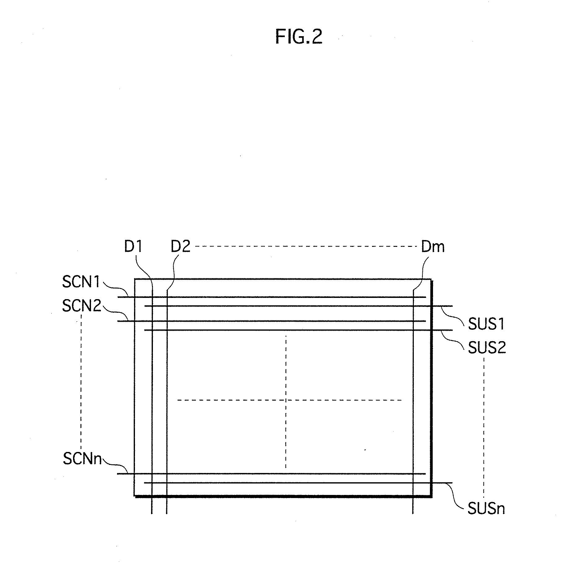
[0072]On one main surface of the front substrate 2, a plurality of scan electrodes SCN1-SCNn and sustain electrodes SUS1-SUSn are arranged alternately in parallel to one another. Each scan electrode makes up a display electrode pair with a corresponding sustain electrode. In a manner to entirely cover the scan electrodes SCN1-SCNn...

working examples

[0134]FIG. 7 illustrates an example setting according to the driving method used by the PDP of the embodiment 1 (working example). According to the setting, the sub-field pattern is changed based on the APL of an image signal to be displayed. Specifically, it is the sub-field converter 18 that effects change of the sub-field pattern.

[0135]The reference numeral “a” in FIG. 7 denotes the sub-field pattern used when the APL of an image signal to be displayed falls within the range of 0 to 1.5%. According to this pattern, the all-cell reset operation is performed only in the reset period of the 1st SF. In the reset periods of the 2nd to 10th SFs, the selective reset operation is performed.

[0136]The reference numeral “b” in FIG. 7 denotes the sub-field pattern used when the APL of an image signal to be displayed falls within the range of 1.5% to 5%. According to this pattern, the all-cell reset operation is performed in the reset periods of the 1st and 4th SFs. In the reset periods of th...

embodiment 2

[0150]FIG. 8 illustrate drive waveforms applied in the all-cell reset period for driving a PDP according to an embodiment 2 of the present invention.

[0151]The embodiment 2 is based on the drive waveforms illustrated in FIG. 4 applied to the respective electrodes of a typical PDP. One feature of the embodiment 2 lies in that an excessive wall voltage erase step is provided between the first and second steps of an all-cell reset period as illustrated in FIG. 8. In the excessive wall voltage erase step, a potential change waveform (voltage change pulse) that rises or falls is applied to the sustain electrodes SUS1-SUSn.

[0152]Regarding the first and second steps of a reset period, the embodiment 2 employs the same sub-field pattern as the embodiment 1. Thus, a description thereof is omitted. The description below relates to the excessive wall voltage erase step that is different from the embodiment 1.

[0153]In FIG. 8A, after the first step of the reset period ends, the voltage Vg (V) is ...


PUM


Abstract

The present invention provides a plasma display panel and a method for driving the plasma display panel each of which ensures to suppress problems associated with an erroneous discharge resulting from accidental occurrence of a strong discharge in a reset period as well as with an address discharge delay. The problems are suppressed without applying an auxiliary erase pulse after the reset period ends. As a result, image display is provided with no flickering and good quality. The reset period includes a first step of applying a voltage having an ascending ramp waveform and a second step of applying a voltage having a descending ramp waveform. Between the first and second steps, a potential change waveform having a rise or fall (voltage change pulse) is applied at least to scan electrodes, sustain electrodes, or address electrodes.

Description

TECHNICAL FIELD[0001]The present invention relates to a plasma display panel apparatus and a method for driving the plasma display panel apparatus. Especially, the present invention relates to a technique of preventing occurrence of an erroneous discharge in a reset period.BACKGROUND ART[0002]A plasma display panel (hereinafter, simply “PDP”) is composed of two panels, namely front and back panels, opposing each other via a plurality of barrier ribs. Between adjacent barrier ribs, red (R), green (G), and blue (B) phosphor layers are disposed. A gap between the two glass panels is filled with a discharge gas and serves as a discharge space. The front panel is provided with a plurality of pairs of display electrodes formed on the glass surface. Each pair of display electrode is composed of a scan electrode and a sustain electrode. The back panel is provided with a plurality of data (address) electrodes formed in parallel to one another on the glass surface. In addition, the address el...

Claims


Application Information

Patent Timeline
IPC IPC(8): G09G3/28G09G3/288G09G3/291G09G3/292G09G3/298
CPCG09G3/2022G09G2310/066G09G3/2927G09G3/292G09G3/296
Inventor AKAMATSU, KEIJIOGAWA, KENJIUEDA, MITSUO
Owner PANASONIC CORP
Why Eureka
Try Eureka