Buried Isolation Layer

a technology of isolation layer and buried junction, which is applied in the direction of semiconductor devices, electrical apparatus, transistors, etc., can solve the problems of increasing undesirable side diffusion, affecting device performance,

Inactive Publication Date: 2009-02-05
INTERSIL INC
View PDF10 Cites 0 Cited by
  • Summary
  • Abstract
  • Description
  • Claims
  • Application Information

AI Technical Summary

Benefits of technology

[0011]The N type device region may be a drain region of a field effect transistor; and a P type body region separates an N type source region from the N type drain region in the substrate

Problems solved by technology

The up diffusion limits the breakdown voltage between the N+ drain contact and the P isolation layer or alters the device performance in some negative manner.
The breakdo

Method used


Image

  • Buried Isolation Layer
  • Buried Isolation Layer
  • Buried Isolation Layer

Examples


Embodiment Construction

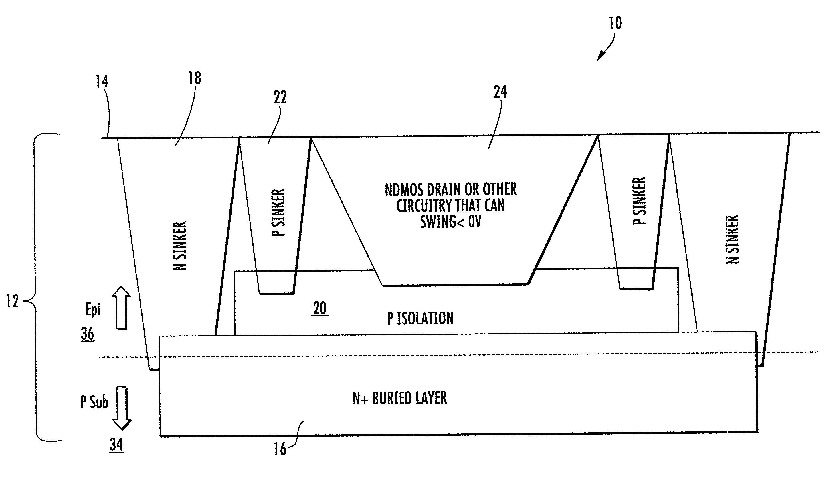
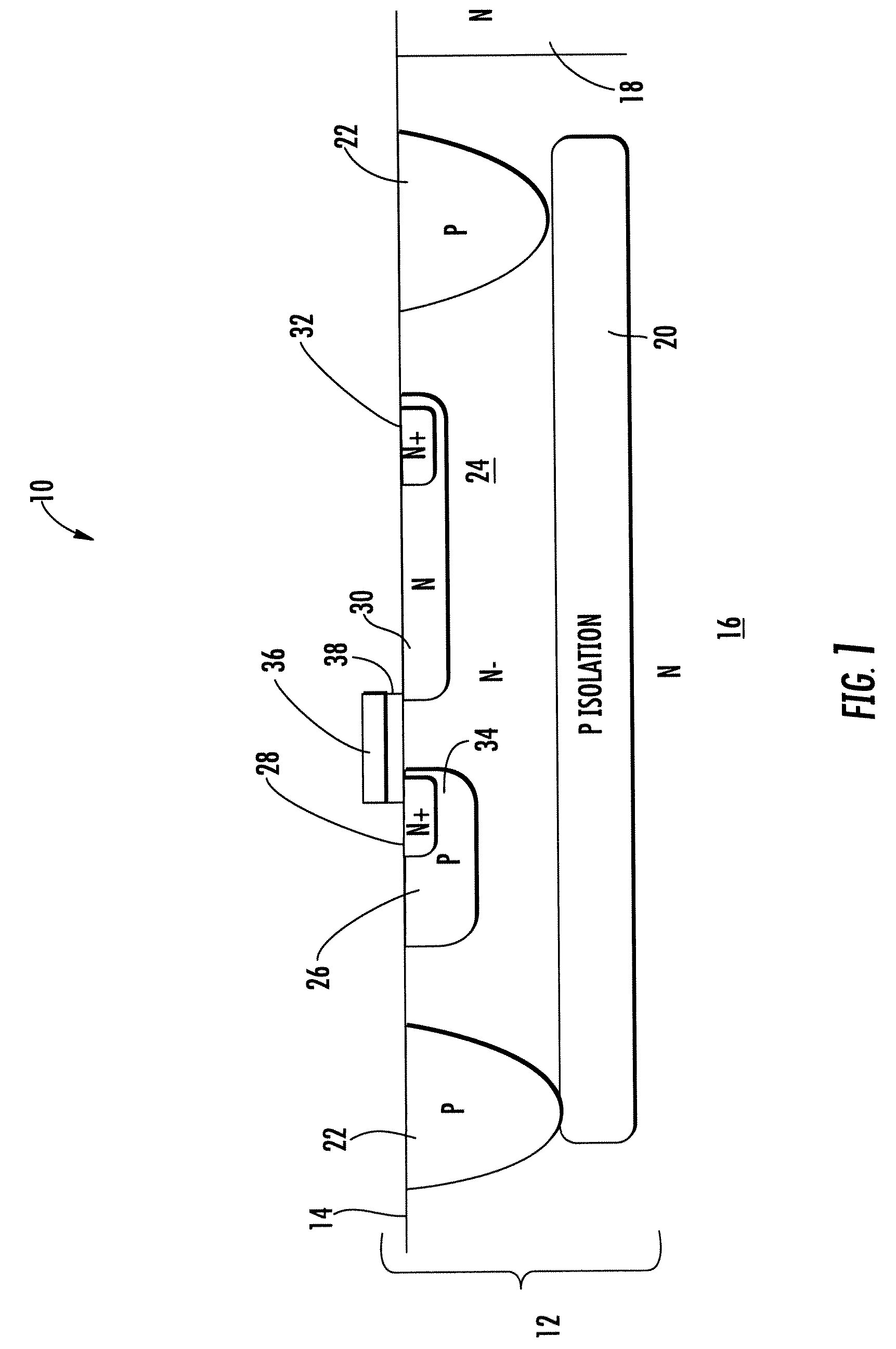
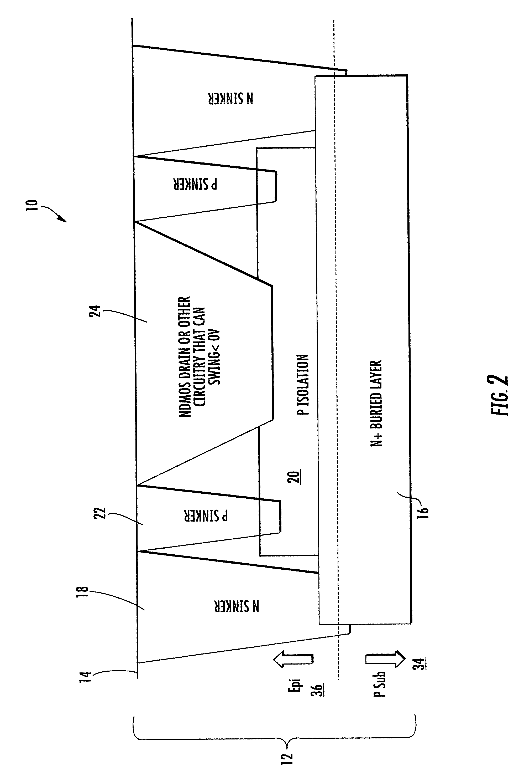
[0016]An integrated circuit 10 of FIGS. 1 through 3 includes a substrate 12 having an N-buried layer 16 with an abutting P isolation layer 20. In FIG. 2, the substrate 12 includes a substrate 34 with an epitaxial layer 36. P contact regions 22 extends from the surface 14 of the substrate down to the P isolation layer 20. In FIGS. 1 and 2, an N contact region 18 extends from the surface 14 of the substrate down to the N buried layer 16. In FIG. 3, the contact to the N buried layer 16 is not shown. The N type device region 24 in FIGS. 1 and 2 and region 42 in FIG. 3 extend from the top surface 14 above the buried P region 20.

[0017]In all embodiments, the P isolation region 20 impurity is indium entirely or partially with some boron. The diffusion coefficient of indium is only about 0.25 that of boron at a given temperature. Consequently up diffusion is significantly reduced. This allows build devices with reduced foot print or die space. Although at least 50% indium is a targeted rang...


PUM


Abstract

The present disclosed integrated circuit includes a substrate having a top surface, a buried N type layer in the substrate, N type contact region extending from the surface to the buried N type region, a buried P type region abutting and above the buried N type region in the substrate, a P type contact region extending from the surface to the buried P type region, and an N type device region in the surface and above the buried P type region. The P type impurity of the buried P type region including an impurity of a lower coefficient of diffusion than the coefficient of diffusion of the impurities of the P type contact region.

Description

BACKGROUND AND SUMMARY[0001]The present disclosure relates to integrated circuit and more specifically to buried junction isolation for integrated circuits.[0002]Subsurface layers are used to define the bottom portion of isolation junctions for many structures in integrated circuits. Multiple layers of alternating conductivity are sometimes stacked vertically to meet the isolation needs of processes such as CMOS and / or DMOS processes used to build mixed signal and power management circuits.[0003]The layers in these processes should be kept as thin as possible while still meeting the required voltages so as to minimize area wasting side diffusion of the edges of the layers.[0004]An example of a critical subsurface layer whose thickness must be minimized is the P isolation layer in the lateral NMOS structure illustrated in FIG. 1. Such a device may be required to provide isolation between the N− region in which the drain is formed and the N layer below the P isolation layer when the N...

Claims


Application Information

Patent Timeline
IPC IPC(8): H01L29/78H01L29/00
CPCH01L21/761H01L29/0878H01L29/7816H01L29/167H01L29/7322H01L29/1083
Inventor CHURCH, MICHAEL
Owner INTERSIL INC
Why Eureka
Try Eureka