Semiconductor laser device structure, thermally assisted magnetic head, and method of manufacturing same

a laser device and laser technology, applied in the direction of mounting head within the housing, special recording techniques, instruments, etc., can solve the problems of lowering the relative positional relationship of attachment accuracy and inability to achieve precise magnetic recording, so as to improve the attachment accuracy and accurate fixation the effect of positional relationship and precise magnetic recording

Active Publication Date: 2009-03-05
TDK CORPARATION
View PDF1 Cites 24 Cited by
  • Summary
  • Abstract
  • Description
  • Claims
  • Application Information

AI Technical Summary

Benefits of technology

[0011]In view of such a problem, it is an object of the present invention to provide a semiconductor laser device structure with an improved attachment accuracy, a thermally assisted magnetic head capable of precise magnetic recording, and a method of manufacturing the same.
[0013]The first alignment mark member is exposed at both the mounting and bonding surfaces and thus can be observed from two directions. While the semiconductor laser device is mounted on the mounting surface of the light source supporting substrate with reference to the first alignment mark member as observed from one direction, the first alignment mark can also be observed from another direction. With reference to the first alignment mark member as observed from the latter direction, the light source supporting substrate can be bonded to the optical waveguide supporting substrate. Namely, though observed from different directions, the same alignment mark member is used for a common reference for two securing operations, whereby attachment errors can be suppressed. Therefore, the laser light emitted from the semiconductor laser device accurately enters the light entrance surface of the optical waveguide and reaches its light exit end.
[0016]Preferably, the exposed surface of the first alignment mark member on the mounting surface is positioned between the second and third alignment mark members, while a fourth alignment mark member embedded within the substrate is exposed at a position separated along a resonator length of the semiconductor laser device from the exposed surface. Arranging a resonator along a line connecting the first and fourth alignment mark members accurately orients the resonator length direction to an area between the second and third alignment mark members.
[0019]Since the first alignment mark member is a common member which can be observed from two directions, bonding with reference to this member can accurately fix the positional relationship between the light exit surface of the resonator and the optical waveguide.
[0020]Since the semiconductor laser device structure in accordance with the present invention has an improved attachment accuracy, the thermally assisted magnetic head using the same enables precise magnetic recording. The manufacturing method in accordance with the present invention can accurately fix the positional relationship between the light exit surface of the resonator and the optical waveguide.

Problems solved by technology

This requires two securing operations, which incur respective attachment errors, thereby lowering the attachment accuracy in the relative positional relationship between the semiconductor laser device and slider.
When the accuracy is low in the laser light advancing direction in a thermally assisted magnetic head in particular, an ultrafine recording area cannot precisely be irradiated with the light, whereby precise magnetic recording may not be achieved.

Method used


Image

  • Semiconductor laser device structure, thermally assisted magnetic head, and method of manufacturing same
  • Semiconductor laser device structure, thermally assisted magnetic head, and method of manufacturing same
  • Semiconductor laser device structure, thermally assisted magnetic head, and method of manufacturing same

Examples


Embodiment Construction

[0027]In the following, a thermally assisted magnetic head as a semiconductor laser device structure in accordance with an embodiment will be explained. The same constituents will be referred to with the same numerals or letters while omitting their overlapping explanations.

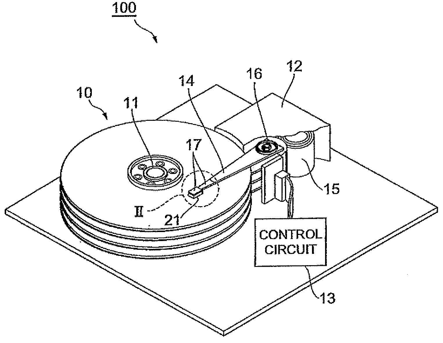
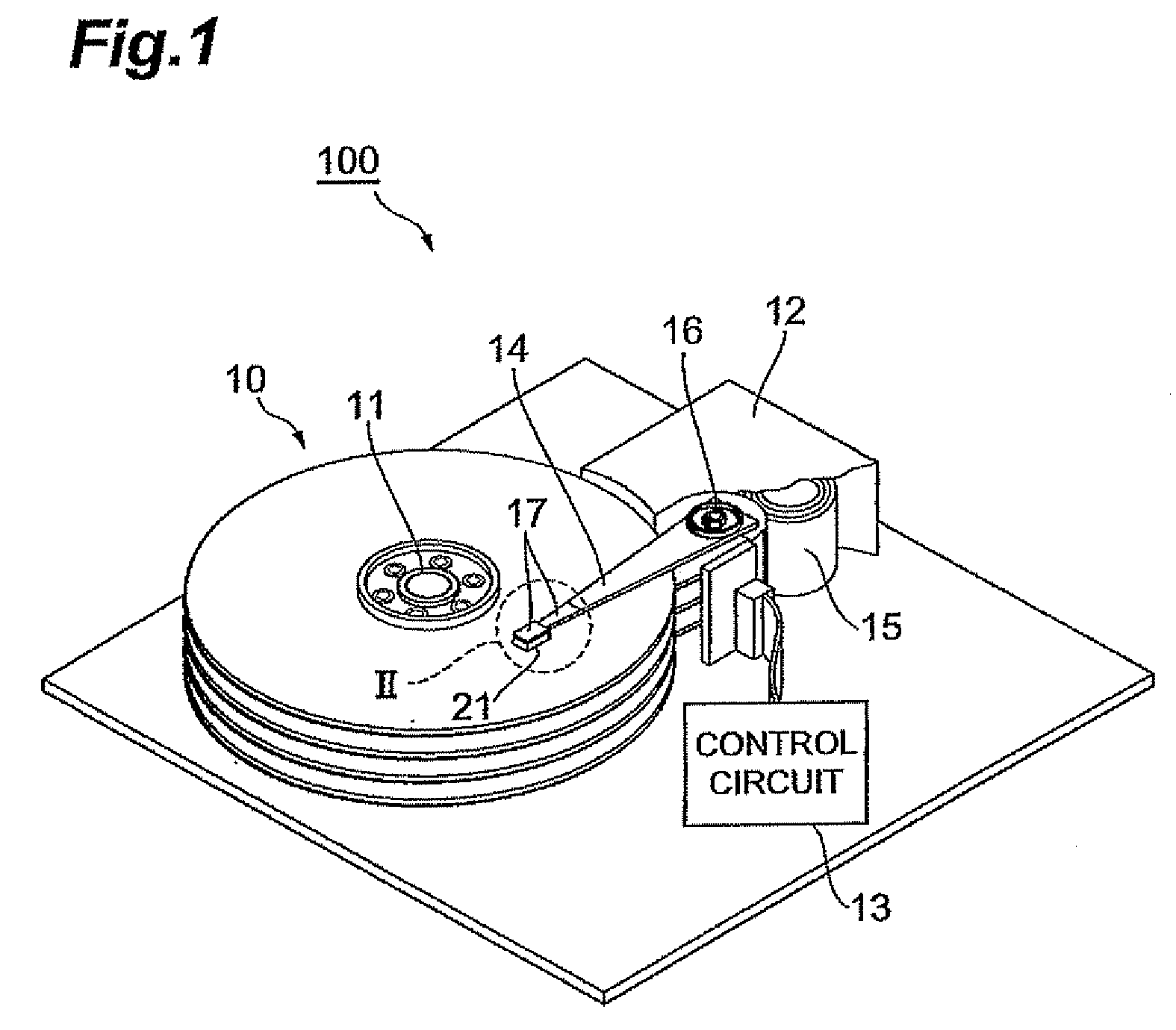
[0028]FIG. 1 is a perspective view of a hard disk drive mounted with the thermally assisted magnetic head in accordance with the embodiment.

[0029]The hard disk drive 100 comprises a plurality of magnetic disks 10 which are magnetic recording media rotating about a rotary shaft of a spindle motor 11, an assembly carriage apparatus 12 for positioning thermally assisted magnetic heads 21 onto tracks, and a read / write and emission control circuit (control circuit) 13 for controlling writing and reading actions of the thermally assisted magnetic heads 21 and regulating a semiconductor laser device (laser diode) which is a light source for generating laser light for thermally assisted magnetic recording.
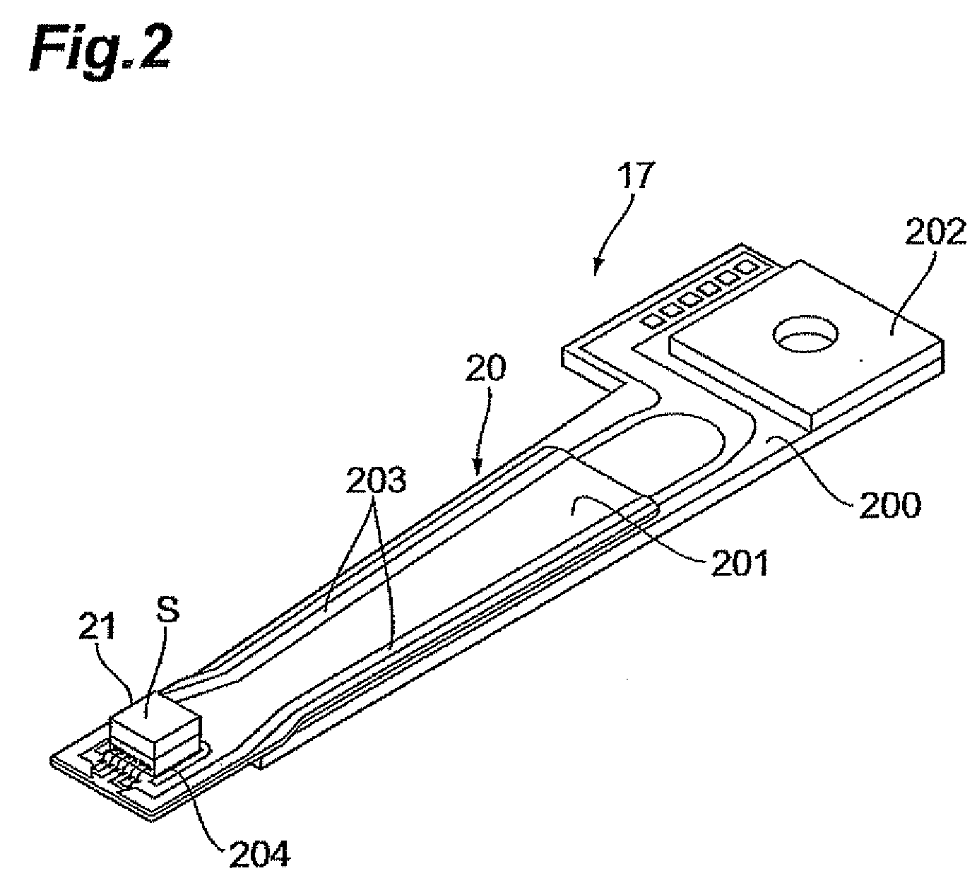
[0030]The assem...


PUM

PropertyMeasurementUnit
lengthaaaaaaaaaa
recording densityaaaaaaaaaa
single-domain structureaaaaaaaaaa

Abstract

A first alignment mark member is exposed at both of a mounting surface and a bonding surface, and thus can be seen from two directions by image sensors. While a semiconductor laser device is mounted on the mounting surface of a light source supporting substrate with reference to the first alignment mark member observed from the direction of the image sensor, the first alignment mark member can also be observed from the direction of the image sensor. With reference to the first alignment mark member observed from the latter direction, the light source supporting substrate is bonded to the slider substrate. Namely, though observed from different directions, the alignment mark member is used for a common reference for two securing operations, whereby attachment errors can be suppressed.

Description

BACKGROUND OF THE INVENTION[0001]1. Field of the Invention[0002]The present invention relates to a semiconductor laser device structure, a thermally assisted magnetic head, and a method of manufacturing the same.[0003]2. Related Background Art[0004]As hard disk dives have been increasing their recording density, thin-film magnetic heads have been required to further improve their performances. As the thin-film magnetic heads, those of composite type having a structure in which a magnetic detecting device such as magnetoresistive (MR) device and a magnetic recording device such as electromagnetic coil device are laminated have been in wide use, while these devices read / write data signals from / onto magnetic disks which are magnetic recording media.[0005]In general, a magnetic recording medium is a sort of discontinuous body in which magnetic fine particles are assembled, while each magnetic fine particle has a single-domain structure. Here, one recording bit is constituted by a plural...

Claims


Application Information

Patent Timeline
Patent Type & Authority Applications(United States)
IPC IPC(8): G11B5/02
CPCG11B5/314G11B2005/0021G11B5/105G11B2005/001
Inventor TANAKA, KOSUKEITO, YASUHIRO
Owner TDK CORPARATION
Why Eureka
Try Eureka