Light Emitting Apparatus and Method of Fabricating the Same

a technology of light emitting apparatus and light emitting film, which is applied in the direction of electric lighting source, solid-state device, electric light source, etc., can solve the problems of increasing the fabrication cost and high cost of circularly polarized light film

Inactive Publication Date: 2009-03-05
SEMICON ENERGY LAB CO LTD
View PDF94 Cites 26 Cited by
  • Summary
  • Abstract
  • Description
  • Claims
  • Application Information

AI Technical Summary

Benefits of technology

[0012]Hence, it is an object of the invention to provide a method of selectively forming a high molecular species material layer which is simpler than using an ink jet method in a light emitting apparatus of an active matrix type using a high molecular species organic compound. Further, it is an object thereof to simply form a structure in which the organic compound layer is not formed at a connection portion of a wiring connected to an outside power source by enabling to selectively form the high molecular species material layer.
[0039]Further, the invention devises a shape of an insulating substance (referred to as bank, partition wall, barrier, embarkment or the like) provided between respective pixels to eliminate a failure in coverage in forming a high molecular organic compound film by a coating method.

Problems solved by technology

Further, according to a light emitting apparatus, there poses a problem that outside scenery is imaged on an observing face (face directed to a side of an observer) by reflecting incident outside light (light outside of the light emitting apparatus) by a rear face of a cathode (face on a side in contact with a luminescent layer) at a pixel which does not emit light.
Further, in order to avoid the problem, it is devised that a circularly polarized light film is pasted on an observing face of the light emitting apparatus to thereby prevent outside scenery from being imaged on the observing face, however, the circularly polarized light film is very expensive and therefore, there poses a problem of an increase in the fabrication cost.

Method used


Image

  • Light Emitting Apparatus and Method of Fabricating the Same
  • Light Emitting Apparatus and Method of Fabricating the Same
  • Light Emitting Apparatus and Method of Fabricating the Same

Examples


embodiment 1

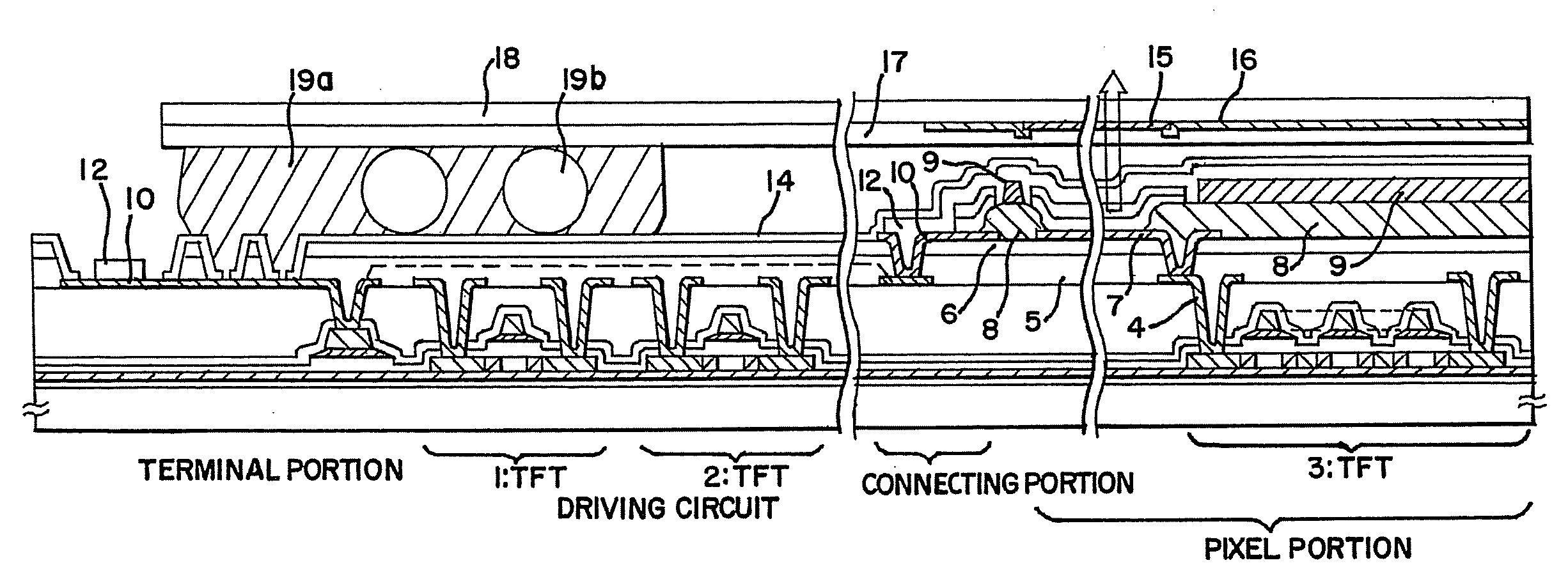
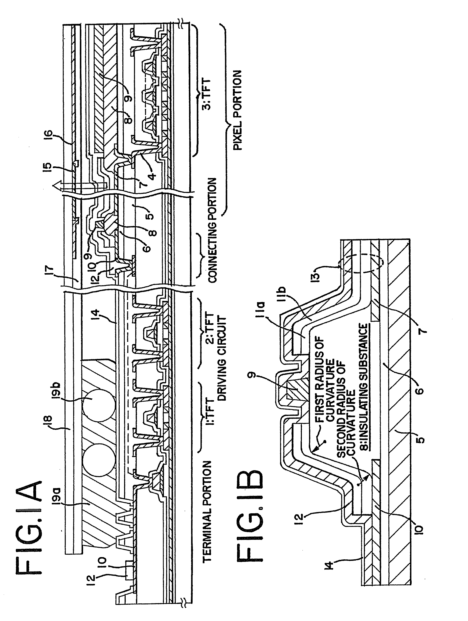
[0075]FIG. 1A shows a sectional view of an active matrix type light emitting apparatus. Here, a luminescent element 13 having a laminated structure comprising a high molecular material for emitting light of white color will be explained as an example.

[0076]In FIG. 1A, a plurality of TFTs 1 through 3 are provided over a substrate having an insulating surface. Further, TFT 1 and TFT 2 are elements constituting portions of a drive circuit portion. Further, TFT3 provided at a pixel portion is an element for controlling current flowing in EL layers 11a and 11b for emitting light of white color and numeral 4 designates a source electrode or a drain electrode. Here, TFT 3 constitutes TFT having a plurality of channels. Further, a channel length L of TFT 3 is preferably equal to or larger than 100 μm. When the channel length L is prolonged, oxide film capacitance Cox is increased and therefore, a portion of the capacitance can be utilized as hold capacitance of an organic luminescent elemen...

embodiment 2

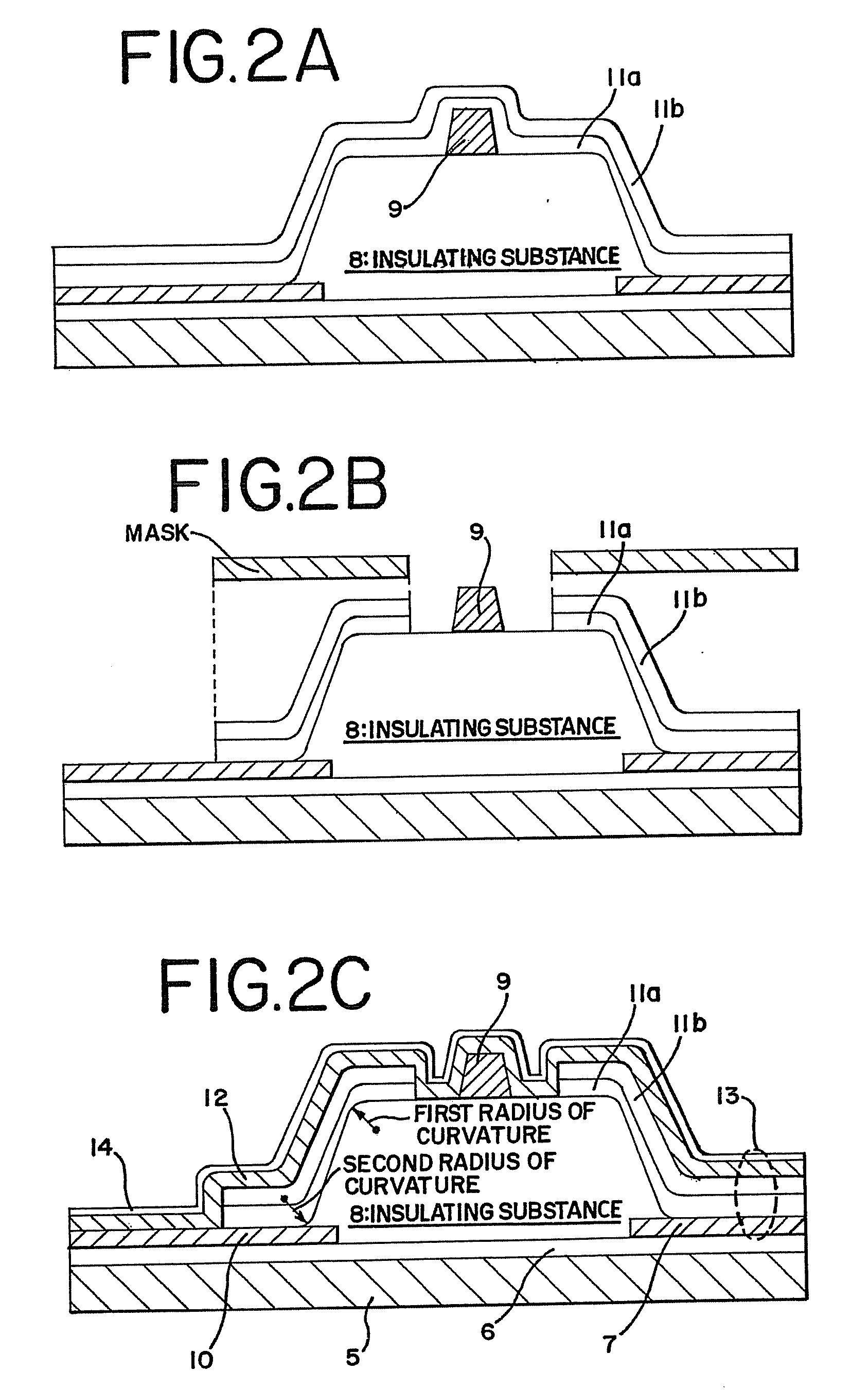
[0094]Here, a simplified explanation will be given as follows of a procedure of forming a luminescent element shown in FIG. 1B in reference to FIGS. 2A, 2B and 2C. Further, for simplification, portions in FIGS. 2A, 2B and 2C the same as those of FIG. 1 designate the same.

[0095]First, TFT (not illustrated here), the first electrode 7, the connection wiring 10, the insulating substance 8 and the third electrode 9 are formed over the substrate, thereafter the organic compound layer 11a is formed by a coating method using spin coating, thereafter sintered by heating in vacuum and successively, the organic compound layer 11b is sintered by heating in vacuum to laminate. (FIG. 2A)

[0096]Successively, etching is carried out selectively by using plasma generated by exciting a single kind or a plurality of kinds of gases selected from the group consisting of Ar, H, F and O. In the etching, the desired region is removed by using a metal mask (FIG. 2B). Although in FIG. 2B, an example in which ...

embodiment 3

[0100]Here, a total of an EL module and arrangement of a drying agent will be explained in reference to FIGS. 3A, 3B and 3C. FIG. 3A is a top view of the EL module. Further, FIG. 3A corresponds to FIG. 1, a sectional view cut by a dotted line A-A′ corresponds to FIGS. 1A and 1B and the same notations are used for the same portions.

[0101]A substrate provided with numerous TFTs (also referred to as TFT substrate) is provided with a pixel portion 40 for display, drive circuits 41a and 41b for driving respective pixels of the pixel portion, a connecting portion for connecting the electrode provided over the EL layer and an extended wiring, a terminal portion 42 for pasting FPC for connecting to outside circuit and a drying agent 44. Further, the drying agent 44c may be arranged such that a total of the drive circuits 41c is concealed by the drying agent 44c as shown by FIG. 3C although the drying agent is arranged to overlap a portion thereof in FIG. 3A and FIG. 3B. Further, the constit...


PUM

PropertyMeasurementUnit
taper angleaaaaaaaaaa
channel lengthaaaaaaaaaa

Abstract

Although an ink jet method known as a method of selectively forming a film of a high molecular species organic compound, can coat to divide an organic compound for emitting three kinds (R, G, B) of light in one step, film forming accuracy is poor, it is difficult to control the method and therefore, uniformity is not achieved and the constitution is liable to disperse. In contrast thereto, according to the invention, a film comprising a high molecular species material is formed over an entire face of a lower electrode connected to a thin film transistor by a coating method and thereafter, the film comprising the high molecular species material is etched by etching by plasma to thereby enable to selectively form a high molecular species material layer. Further, the organic compound layer is constituted by a material for carrying out luminescence of white color or luminescence of single color and combined with a color changing layer or a coloring layer to thereby realize full color formation.

Description

BACKGROUND OF THE INVENTION[0001]1. Field of the Invention[0002]The present invention relates to a light emitting apparatus using a luminescent element emitting fluorescence or phosphorescence by applying an electric field to an element having a film including an organic compound (hereinafter, described as “organic compound layer”) between a pair of electrodes and a method of fabricating the light emitting apparatus. Further, a light emitting apparatus in the specification includes an image display device, a light emitting device or a light source (including illuminating device). Further, a light emitting apparatus includes all of a module of a light emitting apparatus attached with a connector, for example, FPC (Flexible Printed Circuit) or TAB (Tape Automated Bonding) tape or TCP (Tape Carrier Package), a module provided with a printed circuit board at a front end of TAB tape or TCP and a module in which a luminescent element is directly mounted with IC (Integrated Circuit) by COG...

Claims


Application Information

Patent Timeline
Patent Type & Authority Applications(United States)
IPC IPC(8): H01L51/40H01L21/77H01L21/84H01L27/12H01L27/32H01L51/00H01L51/30
CPCH01L27/12H01L27/322H01L27/3246H01L51/0003H01L51/56H01L51/0037H01L51/0042H01L51/005H01L51/0059H01L51/0014H10K59/38H10K71/20H10K59/122H10K71/12H10K85/146H10K85/1135H10K85/60H10K85/631H10K50/824H10K71/00H05B33/14H10K50/805H10K50/85H10K2102/3026
Inventor YAMAZAKI, SHUNPEIMURAKAMI, MASAKAZUSEO, SATOSHI
Owner SEMICON ENERGY LAB CO LTD
Why Eureka
Try Eureka