Memory Element and Method for Manufacturing the Same, and Semiconductor Device

a technology of memory elements and semiconductor devices, applied in bulk negative resistance effect devices, instruments, nanoinformatics, etc., can solve the problems of low material efficiency, large amount of energy consumed in a manufacturing process, and product yield drop, and achieve high yield, high performance and reliability, and excellent performance and reliability.

Inactive Publication Date: 2010-11-11
SEMICON ENERGY LAB CO LTD
View PDF36 Cites 16 Cited by
  • Summary
  • Abstract
  • Description
  • Claims
  • Application Information

AI Technical Summary

Benefits of technology

[0019]In accordance with the present invention, a memory element and a semiconductor device equipped with such a memory element which can be manufactured simply with high yield,

Problems solved by technology

When an organic compound layer is formed by vapor deposition, since only part of the vaporized organic compound is used, which leads to low efficiency in the use of materials.
There are also problems in that for exampl

Method used


Image

  • Memory Element and Method for Manufacturing the Same, and Semiconductor Device
  • Memory Element and Method for Manufacturing the Same, and Semiconductor Device
  • Memory Element and Method for Manufacturing the Same, and Semiconductor Device

Examples


embodiment mode 1

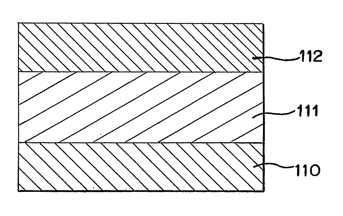
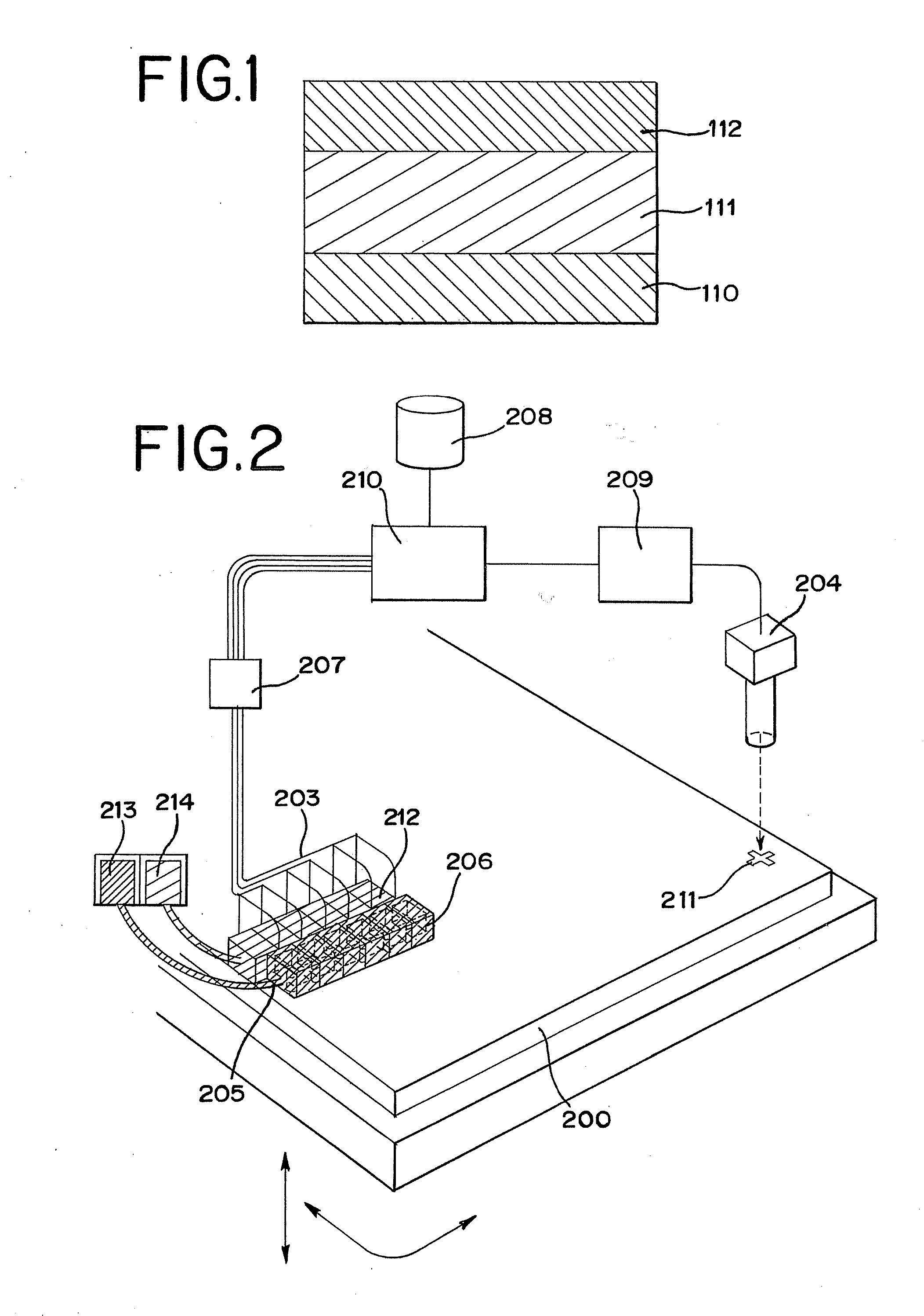
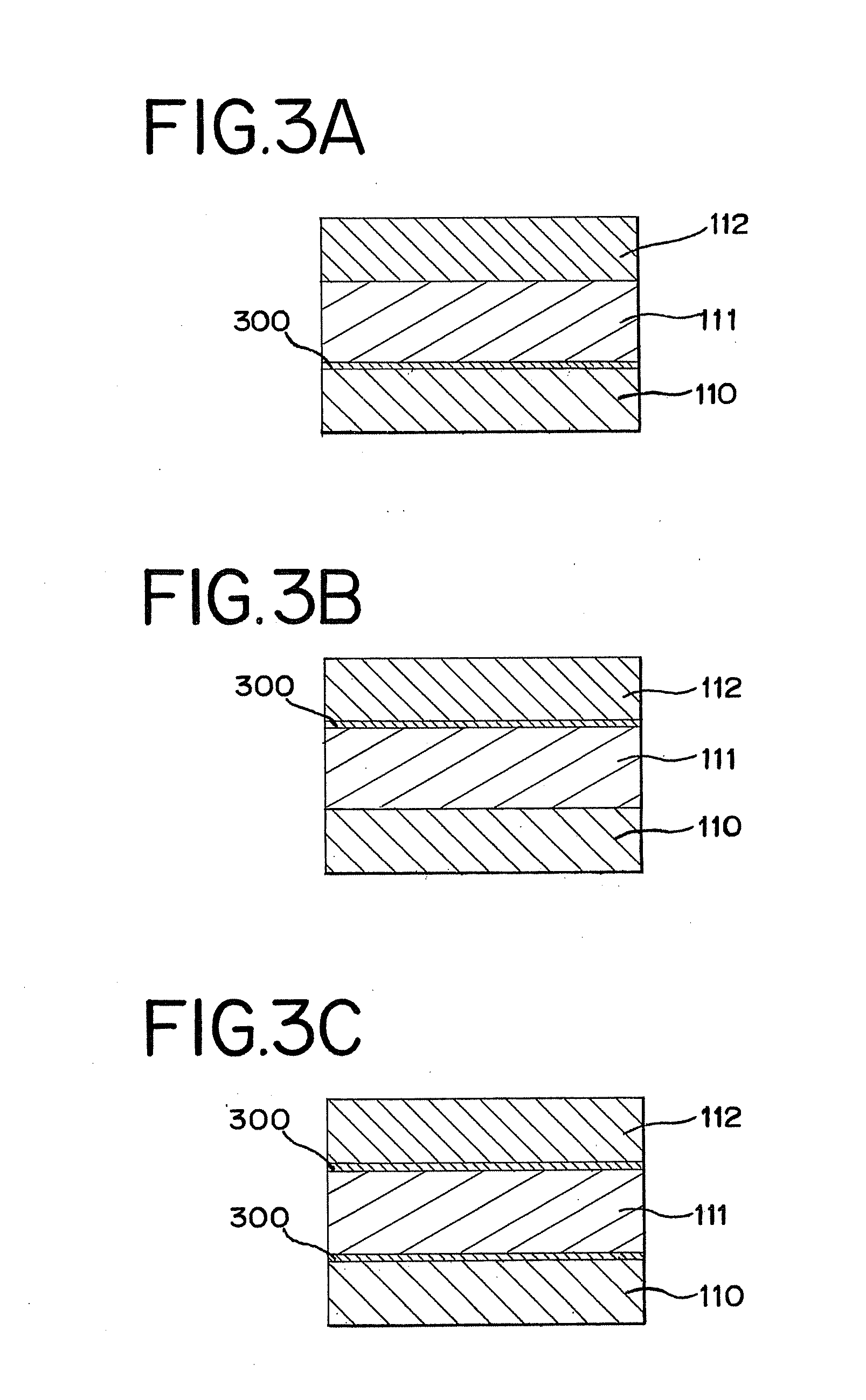
[0041]An example of a structure of a memory element of the present invention will be described with reference to FIG. 1. The memory element shown in FIG. 1 has a structure including a first conductive layer 110, a memory layer 111, and a second conductive layer 112, in which the memory layer 111 is interposed between the first conductive layer 110 and the second conductive layer 112.

[0042]First, an operation mechanism of a memory element of the present invention will be described. The memory layer 111 included in the memory element of the present invention is formed from nanoparticles of a conductive material each of which is coated with an organic thin film. Accordingly, the memory layer 111 is not conductive, and resistance of the memory element is high. When a voltage is applied between the first conductive layer 110 and the second conductive layer 112 of such a memory element, a small amount of current flows through the memory layer 111, so that Joule heat is generated. The Joul...

embodiment mode 2

[0074]This embodiment mode will explain a semiconductor device having a memory element of the present invention, typically a memory device, with reference to the drawings. Note that this embodiment mode will show a case where the structure of the memory device is a passive matrix type.

[0075]FIG. 4A shows a structural example of a semiconductor device shown in this embodiment mode. A semiconductor device 400 includes a memory cell array 411 where memory elements 401 are arranged in matrix, decoders 412 and 413, a selector 414, and a readout / write circuit 415. The structure of the semiconductor device 400 which is shown here is only one example and the semiconductor device 400 may also include other circuits such as a sense amplifier, an output circuit, or a buffer.

[0076]The decoders 412 and 413, the selector 414, the readout / write circuit 415, an interface, and the like may also be formed over a substrate as with the memory element. Alternatively, they may be attached externally as I...

embodiment mode 3

[0104]This embodiment mode will explain a semiconductor device having a memory element of the present invention with reference to FIGS. 7A to 7C. Specifically, this embodiment mode will explain an active-matrix memory device.

[0105]FIG. 7A shows a structural example of a semiconductor device shown in this embodiment mode. A semiconductor device 700 includes a memory cell array 711 where memory cells 701 are arranged in matrix, decoders 712 and 713, a selector 714, and a readout / write circuit 715. The structure of the semiconductor device 700 which is shown here is only one example and the semiconductor device 700 may also include other circuits such as a sense amplifier, an output circuit, or a buffer.

[0106]The decoders 712 and 713, the selector 714, the readout / write circuit 715, an interface, and the like may also be formed over a substrate as with a memory element. Alternatively, they may be attached externally as IC chips.

[0107]The memory cell 701 includes a first wiring connecte...


PUM


Abstract

The memory element has a structure at least including a first conductive layer, a second conductive layer, and a memory layer disposed between the first conductive layer and the second conductive layer. The memory layer is formed by a droplet discharge method using nanoparticles of a conductive material each of which is coated with an organic thin film. Specifically, a composition in which nanoparticles of a conductive material each of which is coated with an organic thin film are dispersed in a solvent is discharged (ejected) as ink droplets, and the solvent is dried to be vaporized to form the memory layer. Accordingly, a memory element can be formed simply. In addition, efficiency in the use of materials can be improved and yield is also improved, so that the memory element can be provided at low cost.

Description

TECHNICAL FIELD[0001]The present invention relates to a memory element and a semiconductor device having the memory element.BACKGROUND ART[0002]In recent years, a semiconductor device having various functions, in which a plurality of circuits is integrated over an insulating surface, has been developed. In addition, a semiconductor device capable of transmission and reception of data, which is provided with an antenna and operates with electric energy into which electric wave received by the antenna has been converted, is developed. Such a semiconductor device is referred to as a wireless chip (also referred to as an ID tag, an IC tag, an IC chip, an RF (radio frequency) tag, a wireless tag, an electronic tag, or an RFID (radio frequency identification)), and has already been introduced into some markets.[0003]Most of such semiconductor devices that have already been put into practical use generally have an antenna and a circuit (referred to as an IC (integrated circuit) chip) using...

Claims


Application Information

Patent Timeline
IPC IPC(8): H01L45/00H01L21/02
CPCB82Y10/00G11C13/00G11C13/0014G11C2213/77G11C2213/79H01L27/101H01L45/145H01L27/11206H01L27/12H01L27/1203H01L27/1214Y10S977/773H01L27/112H10B20/00H10B20/20H10N70/883
Inventor YOSHIZUMI, KENSUKE
Owner SEMICON ENERGY LAB CO LTD
Why Eureka
Try Eureka