Unlock instant, AI-driven research and patent intelligence for your innovation.

Memory access control device, command issuing device, and method

a memory access control and command issuing technology, applied in the direction of instruments, computing, electric digital data processing, etc., can solve the problems of not driving data signals, and reducing the efficiency of accessing memory

Inactive Publication Date: 2009-04-09
CANON KK
View PDF5 Cites 2 Cited by
  • Summary
  • Abstract
  • Description
  • Claims
  • Application Information

AI Technical Summary

Benefits of technology

[0052]The present invention has as an object to access memory efficiently.

Problems solved by technology

However, as operating frequencies rise, keeping the wiring delay from exceeding one clock cycle of the memory through substrate design has become difficult, and cases arises in which memory devices have differing access latencies.
If a command is issued without satisfying the command issuing interval calculated using the above calculation method, there is the risk of collision between the driving of the data signals between the memory access control circuit 100 and the memory devices 191 and 192.
A situation can arise in which data signals are not driven due to excessive gaps in the command issuing intervals, even when accessing memory devices with low access latency.
Accordingly, a problem arises in that unnecessary transfer intervals are wasted during cycles in which data transfer is possible, lowering usage efficiency of the memory bus.

Method used


Image

  • Memory access control device, command issuing device, and method
  • Memory access control device, command issuing device, and method
  • Memory access control device, command issuing device, and method

Examples


first embodiment

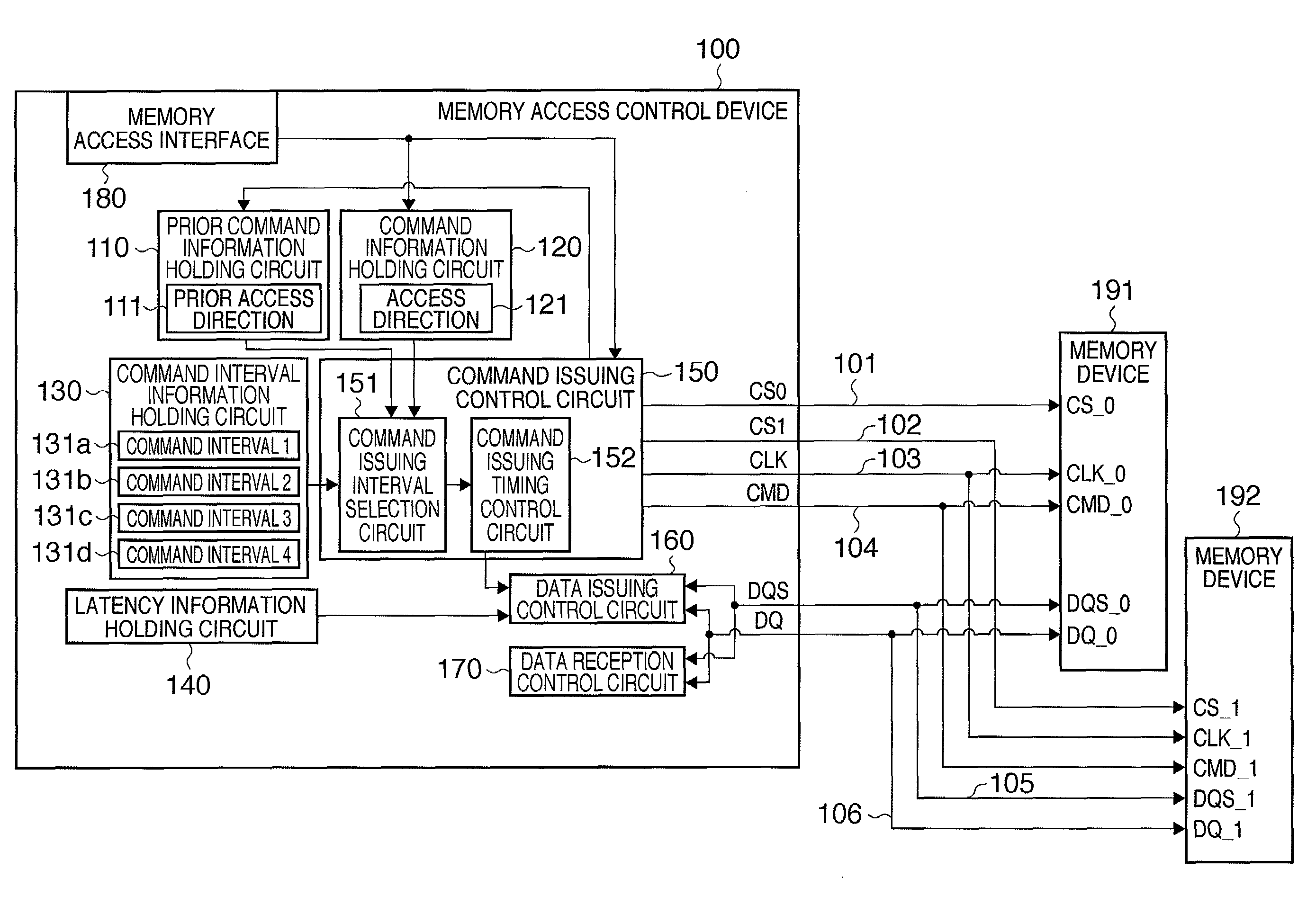
[0065]FIG. 4 is a block diagram showing one example of a memory access control circuit according a first embodiment. As shown in FIG. 1, two memory devices 591 and 592 are connected to a memory access control device 500, and the memory access control device 500 controls access to the memory devices 591 and 592.

[0066]In the first embodiment, too, DDR-type memory devices are used as the memory devices. Description of signals 501 to 506 between the memory access control device 500 and the memory devices 591 and 592 is omitted, as these signals are the same as the signals 101 to 106 described using FIG. 1.

[0067]In the memory access control device 500, 510 is a prior command information holding circuit, and holds information on the command issued immediately before. The prior command information holding circuit 510 is internally provided with a prior access direction buffer 511 for holding the reading or writing direction of the command issued immediately before and a prior access device...

second embodiment

[0107]Next, a detailed described is given of a second embodiment according to the present invention with reference to the drawings. In the first embodiment, minimum command interval values are held in the command interval buffers 531a to 531N, but in the second embodiment, they are calculated when issuing the next command.

[0108]FIG. 8 is a block diagram showing one example of a memory access control circuit according a second embodiment. As shown in FIG. 8, a memory access control device 900 is connected to memory devices 991 and 992, and controls access to the memory devices 991 and 992.

[0109]In the second embodiment, too, DDR-type memory devices are used as the memory devices. Description of signals 901 to 906 between the memory access control device 900 and the memory devices 991 and 992 is omitted, as these signals are the same as the signals 501 to 506 described using FIG. 4.

[0110]In the memory access control device 900, 910 is a prior command information holding circuit, and h...


PUM


Abstract

A memory access control device for controlling access to a plurality of memory devices with differing latency, controls, when performing a first access and then a second access, the timing of performing the second access, according to a memory device accessed in the first access and a memory device accessed in the second access.

Description

BACKGROUND OF THE INVENTION[0001]1. Field of the Invention[0002]The present invention relates to memory access control technology for controlling access to a plurality of memory devices with differing latency.[0003]2. Description of the Related Art[0004]Conventionally, substrates are designed such that wiring delay between large-scale integrated circuits (LSIs) and memory devices does not exceed one clock cycle of the memory. However, as operating frequencies rise, keeping the wiring delay from exceeding one clock cycle of the memory through substrate design has become difficult, and cases arises in which memory devices have differing access latencies.[0005]Accordingly, memory access control circuits capable of accurately performing data exchange with a plurality of memory devices taking into consideration wiring delay have been considered (e.g., Japanese Patent Laid-Open No. 2003-173290).[0006]FIG. 1 is a block diagram showing one example of a memory access control circuit in a con...

Claims


Application Information

Patent Timeline
IPC IPC(8): G06F12/00
CPCG06F12/00G06F13/4243
Inventor OCHIAI, WATARU
Owner CANON KK
Features
  • R&D
  • Intellectual Property
  • Life Sciences
  • Materials
  • Tech Scout
  • Unparalleled Data Quality
  • Higher Quality Content
  • 60% Fewer Hallucinations
Learn More